LNW80 Technical Reference Manual
THEORY OP OPERATIONS
LNW80 BOARD
SYSTEM CLOCK
The system clock is a 16MHz oscillator utilizing Yl
and U1 to form a series resonant circuit. U87, a
synchronous 4-bit counter, is used to perform the divide by
four for the 4MHz and a divide by nine for the 1.77MHz CPU
operation. When the HI/LO switch is depressed, the signal
FORCELO* (U29-5) is a logic "0" resulting with a preset of
1,0,0 at U87 pins 3,4, and 5 respectively. This preset will
program U87 to divide by nine resulting in a 1.77MHz CPU
clock at U2-6.
During 4MHz operation, U87 will be preset with 0,1,1
at pins 3,4, and 5 respectively resulting in a divide by
four of the system clock. At 4MHz, the signal NHI* (U15-2)
will be a logic "0". Thus when ROMRD* (U15-1) is active, a
WAIT* will be generated through U31 to the CPU pin 24
allowing for the relatively slow access time of the ROM.
During automatic switching (SW1=1) when the floppy
address (37EC) is decnded along with a logic "0" at INREQ*,
the one-shot at U120 will be triggered forcing U120-4 low.
This results with a logic "0" at U29-4 resulting in a CPU
speed of 1.77MHz as when the HI/LO switch was depressed.
The clock speed will remain at this state until the one-shot
expires at which time the CPU automatically and
synchronously returns to 4MHz.
CPU ADDRESS LINES
The Z80A provides 16 address lines which define the
64K of addressable memory locations. These address lines
are buffered from the Z80A through U3 and U5. U3-1 and U5-1
should be a logic "0" thus enabling their outputs at all
times. The upper addresses are latched through U5, an
LS373, to prevent the address from changing prematurely.
During refresh time, the lower 7 bits contain a valid
refresh address.
CPU DATA BUS
The CPU utilizes an 8-bit bidirectional data bus.
The data bus is used for data exchanges with memory and I/0
devices. The data is buffered through U4 and U17. DBIN
(U1-10) is used for directional control. When DBIN is a
logic "1" the CPU is receiving data. When DBIN is low the
CPU is sending data.
WAIT*, INT*, and TEST*
The WAIT* input to the Z80A CPU will cause the Z80A
to extend its cycle, resulting in slowing down the CPU. The
LNW80 utilizes one WAIT function when a ROM read is in
process and one or two waits when accessing the video
memory. These waits are required in the hi-speed mode of
4MHz to ensure data validity when accessing the slower
memory devices. There are no wait states when accessing the
program memory (RAM) on the LNW80 (requiring 200ns or faster
RAM's).
The wait term is generated by U31. U31-3, the
clock, is delayed by U16. This clock delay results in
proper data setup time to U31. U61-3 is WAITHLD. This will
increase the wait from the usual one wait state for the
Level II ROM's, to multiple wait states when reading from
the video memory. Pin 33 of J1 is the bus WAIT signal.
This input may be utilized by other external devices that
may wish to pose a wait condition on the Z80A procesor.
The INT* signal is a maskable interrupt to the ZBHA
pin 16. The Level II Basic ROM utilizes interrupt mode 1.
When the CPU is interrupted, a restart to 1ocation 0038H is
executed.
Pin 23 of J1 is TEST* which is a busrequest signal
to the Z80A CPU. The CPU responds by tri-stating its data,
address and output control signals. Since the Z80A CPU is
fully buffered, all the buffers (U3, U4, U5, U17, and U18)
will also be tri-stated. Once these buffers are tri-stated,
any device on the expansion bus may control the function of
the LNW80 board. One important consideration is that the
dynamic program RAM's are refreshed by the Z80A processor.
Therefore, any controlling device on the expansion bus must
consider memory refresh.
CPU CONTROL SIGNALS
The ZRD* signal is a tri-state output, active low.
ZRD* indicates that the CPU is ready to receive data from
memory or an I/0 device. It is input to U36 pins 4 and 12.
When U36-12 goes low it enables DBIN. When ZRD* and ZMREQ*
go low, they enable IRD* (U36-6). RDOUT* will also be
enabled if RDWRDIS (U51-8) is true. Note that RDWRDIS is
used to disable the lower 16K when the HI RESOLUTION
GRAPHICS RAM are enabled.
ZWR* indicates that the CPU holds valid data to be
stored in memory or an I/O device. When ZWR* and ZMREQ*
both go low, IWR* (U36-3) is enabled. WROUT* (U36-1I) will
also be enabled if RDWRDIS is true.
ZMREQ* indicates that the address bus holds a valid
address for a read or write operation. Note that it is also
used far memory refreshing.
ZIORQ* indicates that the lower half of the address
bus holds a valid I/0 address for an I/0 read or write
operation. It is used as the enable at U35-15. When
combined with a WR*, IOUT* will be enabled (U35-9). When
ZIORQ* is combined with a RD*, IIN* will be enabled
(U35-11). ZIORQ* is also combined with ZM1* when an
interupt is being acknowledged.
RFSH* indicates that the lower 7 bits of the address
contains a refresh address for dynamic memories and the
current MREQ* signal is used to do a refresh read to all
dynamic memories. Note that it is used to clear U46-5
during refresh time. Resulting in the selection of the
lower seven address lines and a logic "1" far the CAS*
signal.
ADDRESS DECODING CIRCUIT
The address decoding circuit consists of U6 and U35.
The decoding circuit uses the higher order address bits to
enable the locations within the memory map which the CPU
wishes to access. U6 is a 3 to 8 line decoder. It uses A15
and IMREQ* as enables and A12, A13, and A14 as inputs.
Refer below far a listing of the memory mapped sections of
the LNW80 along with their decoded addresses.
LNW80 MEMORY MAP
ADDRESS
DECIMAL HEX DEVICE
==================================================
0 0
12288 3000 BASIC ROM
==================================================
12289 3001
14301 37DD UNUSED
==================================================
14302 37DE COMMUNICATION STATUS ADDRESS
14303 37DF COMMUNICATION DATA ADDRESS
14304 37E0 INTERUPT BATCH ADDRESS
14305 37E1 DISK DRIVE SELECT LATCH
14308 37E4 CASSETTE SELECT LATCH
14312 37E8 PARALLEL PAINTER ADDRESS
14316 37EC FLOPPY DISK CONTROLLER ADDRESS
==================================================
14336 3800
14591 38FF KEYBOARD
==================================================
15360 3C00
16383 3FFF LO-RES VIDEO RAM
==================================================
16384 4000
32767 7FFF 16K PROGRAM RAM
==================================================
32768 8000
65535 FFFF 32K RAM (EXPANSION BOARD)
==================================================
ROM
The LNW80 ROM consists of six EPROMs. ROMA is
memory mapped from 0 to 2K, ROMA1 from 2K to 4K, ROMB from
4k to 6K, ROMB1 from 6K to 8K, ROMC from 8K to 10K, and
ROMC1 from 10K to 12K.
Each ROM has three enables. Pin 21 is an active
high enable and pins 18 and 28 are active low enables. Pin
21 is pulled high on all ROMs with 33 ohm pull-up
resisters.
ROMA and ROMA1, pins 28 are enabled by "0-4K*"
(U6-15). "8-4K*" goes low when U6 pins 1,2,3,4, and 5 are
at logic levels "0","0","0","0, and "0" respectively. RA11
is inverted at U58-8 and enables either ROMA and ROMA1 at
pins 18.
ROMB and ROMB1, pins 28 are enabled by "4-8K*"
(U6-14). 4-8K* goes low when U6 pins 1,2,3,4, and 5 are
at logic levels "1","0","0","0", and "0" respectively. RA11
enables either ROMB or ROMB1 at pins 18.
ROMC and ROMC1, pins 20 are enabled by "8-12K*"
(U6-13). "8-12K*" gees low when U6 pins 1,2,3,4, and 5 are
at logic levels "0 ,"1","0","0", and "0" respectively. RA11
enables ROMC or ROMCl at pins 18.
Addresses A0 through A11 are buffered through U62
and U65, LS244's. The data bus out is buffered through U63
and is enabled by "RAM/ROM*" (U52-6). "RAM/ROM*" goes low
when RD* occurs with either "0-4K*", "4-8K*", or "8-12K*".
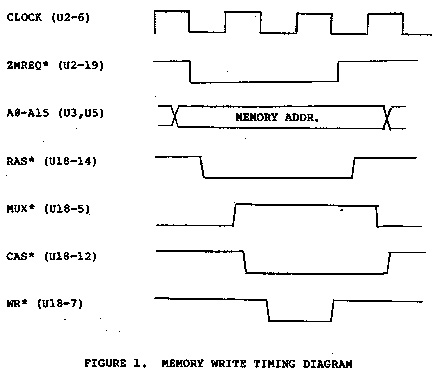
PROGRAM RAM
The LNW80 utilizes the 16Kx1 dynamic memories (4116
type) with maximum access time of 200ns. The 14 address
lines are multiplexed into the 7 address inputs. The
addressing sequence is RAS* (Row Address Select), MUX
(Multiplex), and then CAS* (Column Address Select). The
timing diagram for a write operation of the memory control
signals is displayed in the following diagram. The RAM data
bus out is enabled by "RAM/ROM*" at U63 when RAM* is decoded
at U19-6 during a read operation.
 RAM REFRESH
Dynamic RAM require periodic refreshing to retain
data information. If the system does not receive periodic
refreshing the dynamic RAMs will begin to "forget" data.
The LNW80 utilizes the Z80A CPU to generate the
refresh to the RAN's. The memory refresh address is output
on the lower 7 address bits during refresh time. An
instruction fetch will increment the refresh register.
The LNW80 uses a "RAS*" only refresh, where RAS*
will be low and CAS* will be high during refresh. At
refresh time MUX will be low selecting AB-A7 as the RAM
address.
KEYBOARD
The LNW80 keyboard is designed specifically for the
LNW80 computer providing a 62 keypad, an 11 key numeric
keypad, and all the special functions that are available to
you through the LNW80 computer.
The keyboard is a scanning type keyboard based on an
eight by eight matrix. Normally, all lines are floating
until the KYBD* signal goes law which turns Q1 an and pulls
all signals high indicating a keyboard scan operation.
KYBD* is decoded through U35 when a keyboard address is
placed on the address bus and RD* is active.
Note that lower case is enabled only with software
driver routines such as those available in DOS+, NEWDOS80,
and ELECTRIC PENCIL.
SPECIAL KEYBOARD FUNCTIONS
RESET (RST): Both RST keys must be depressed to reset
the computer.
HIGH LOW: Forced LOW Speed switch. When depressed
the system will operate in LOW speed.
Otherwise the system will operate in
forced high speed.
CONTROL: This is a special software controlled key.
It is used in software such as the
ELECTRIC PENCIL ward processing program.
CAPS LOCK: Disables lower case characters.
Fl, F2: User definable keys. Needs special
software driver.
VIDEO DIVIDER CHAIN
The video divider chain provides the necessary logic
for video processing, including video ram addressing, and
vertical and horizontal timing pulses. The basis of the
video divider chain is the 10.738MHz clock at U119-6. This
signal appears as a sine wave and is exactly 3 times the
color frequency of 3.579MHz. U121 executes a divide by 2.
This results in 2 input frequencies to the divider chain at
U122.
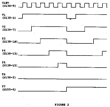
In the standard 64 character mode, 32CHAR*(U122-1)
will be high so that the 8 inputs to U122 will be selected
therefore the clock input at U138-9, CLKT, will be
10.738MHz. U138 provides the basic timing signals for video
processing. Figure 2 represents a timing diagram for the
outputs of U138 and U155 in the 64 character mode.
RAM REFRESH
Dynamic RAM require periodic refreshing to retain
data information. If the system does not receive periodic
refreshing the dynamic RAMs will begin to "forget" data.
The LNW80 utilizes the Z80A CPU to generate the
refresh to the RAN's. The memory refresh address is output
on the lower 7 address bits during refresh time. An
instruction fetch will increment the refresh register.
The LNW80 uses a "RAS*" only refresh, where RAS*
will be low and CAS* will be high during refresh. At
refresh time MUX will be low selecting AB-A7 as the RAM
address.
KEYBOARD
The LNW80 keyboard is designed specifically for the
LNW80 computer providing a 62 keypad, an 11 key numeric
keypad, and all the special functions that are available to
you through the LNW80 computer.
The keyboard is a scanning type keyboard based on an
eight by eight matrix. Normally, all lines are floating
until the KYBD* signal goes law which turns Q1 an and pulls
all signals high indicating a keyboard scan operation.
KYBD* is decoded through U35 when a keyboard address is
placed on the address bus and RD* is active.
Note that lower case is enabled only with software
driver routines such as those available in DOS+, NEWDOS80,
and ELECTRIC PENCIL.
SPECIAL KEYBOARD FUNCTIONS
RESET (RST): Both RST keys must be depressed to reset
the computer.
HIGH LOW: Forced LOW Speed switch. When depressed
the system will operate in LOW speed.
Otherwise the system will operate in
forced high speed.
CONTROL: This is a special software controlled key.
It is used in software such as the
ELECTRIC PENCIL ward processing program.
CAPS LOCK: Disables lower case characters.
Fl, F2: User definable keys. Needs special
software driver.
VIDEO DIVIDER CHAIN
The video divider chain provides the necessary logic
for video processing, including video ram addressing, and
vertical and horizontal timing pulses. The basis of the
video divider chain is the 10.738MHz clock at U119-6. This
signal appears as a sine wave and is exactly 3 times the
color frequency of 3.579MHz. U121 executes a divide by 2.
This results in 2 input frequencies to the divider chain at
U122.
In the standard 64 character mode, 32CHAR*(U122-1)
will be high so that the 8 inputs to U122 will be selected
therefore the clock input at U138-9, CLKT, will be
10.738MHz. U138 provides the basic timing signals for video
processing. Figure 2 represents a timing diagram for the
outputs of U138 and U155 in the 64 character mode.
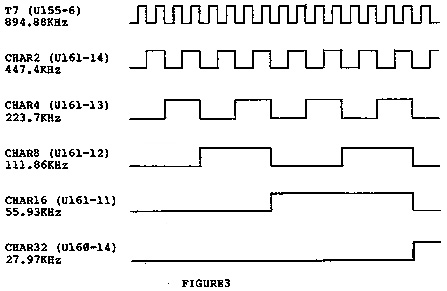
 During 64 character mode, T7* is selected as the
control clock(CNTRCLK) for the video timing chain(U122-12).
The circuitry of U138 and U155 effectively produces a divide
by 12 such that T7* is 10.738MHz/12 or 894.8KHz. Note also
that T7 is selected as CHAR1(U122-9). CNTRCLK is the clock
input to U168 and U161(S161's). Figure 3 illustrates the
outputs of U168 and U161.
During 64 character mode, T7* is selected as the
control clock(CNTRCLK) for the video timing chain(U122-12).
The circuitry of U138 and U155 effectively produces a divide
by 12 such that T7* is 10.738MHz/12 or 894.8KHz. Note also
that T7 is selected as CHAR1(U122-9). CNTRCLK is the clock
input to U168 and U161(S161's). Figure 3 illustrates the
outputs of U168 and U161.
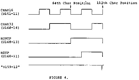
 Note that HORTP(U160-13) is not half the frequency
of CHAR32(U168-14). T6INH*(U155-9) prevents the completion
of its period by clearing U160 and U161 at the end of each
horizontal line. The frequency of HORTP is 15.750KHz
resulting in a period of 63.49us for each line.
Each line consists of 112 characters. Allowing one
CHAR1 period for each 2 characters the time span for 112
characters is 62.58us. Note that we are left with 0.91us at
the end of each horizontal line. T6INH* is used to delay
the timinq chain to "waste" this additional time before
starting the next cycle. U167 is used to add the additional
delay in T6INH*. It is ANDed with T6 at U154 thus delaying
T6*(U154-8) from clearing U138.
HSTP(U168-11) is the ORing of CHAR16 and CHAR32,
ANDed with HORTP. This is the horizontal sinc timing pulse.
Its frequency is 15.750KHz. Refer to figure 4 for the
timing diagram.
U159-12 is also displayed in figure 4. It goes low
after the 112th character and also has a frequency of
15.750KHz. It serves 2 important purposes. 1st, it is the
data input to U124 which when clocked clears U155 and thus
enabling T6INH*. Also it is the input to U156-13 and thus
increments the row count.
Note that HORTP(U160-13) is not half the frequency
of CHAR32(U168-14). T6INH*(U155-9) prevents the completion
of its period by clearing U160 and U161 at the end of each
horizontal line. The frequency of HORTP is 15.750KHz
resulting in a period of 63.49us for each line.
Each line consists of 112 characters. Allowing one
CHAR1 period for each 2 characters the time span for 112
characters is 62.58us. Note that we are left with 0.91us at
the end of each horizontal line. T6INH* is used to delay
the timinq chain to "waste" this additional time before
starting the next cycle. U167 is used to add the additional
delay in T6INH*. It is ANDed with T6 at U154 thus delaying
T6*(U154-8) from clearing U138.
HSTP(U168-11) is the ORing of CHAR16 and CHAR32,
ANDed with HORTP. This is the horizontal sinc timing pulse.
Its frequency is 15.750KHz. Refer to figure 4 for the
timing diagram.
U159-12 is also displayed in figure 4. It goes low
after the 112th character and also has a frequency of
15.750KHz. It serves 2 important purposes. 1st, it is the
data input to U124 which when clocked clears U155 and thus
enabling T6INH*. Also it is the input to U156-13 and thus
increments the row count.
 Each character position consists of a 6x12 matrix.
Six dots and 12 horizontal rows. UX56 increments by one
after each horizontal scan. When the row count is equal to
12, V168-3 will go high thus clearing U156 setting the row
count back to zero and also clocking U153-11 and
incrementing the line count by one.
Note that the screen consists of 22 lines (only 16
are displayed) and each line has 12 rows. LINE1, the least
siqnicicant bit of the line counter, changes state every 2nd
line and thus has the same period as 24 rows or 24x63.49us
or 1.524ms. Its frequency is therefore 656.3Hz. Using
similar logic, you can find that LINE2=328.1Hz,
LINE4=164.1Hz, and LINES=82.8Hz.
A similar situation exists for VERTP(U156-6) as did
for HORTP in that U156 is cleared before VERTP, which
represents line16, completes its full period. When the
total line count is 22 the inputs to U169 pins 3,4 and 5 are
high, thus its output pin6 clears the line count back to
zero. In 22 lines LINE1 changes state 3.1 times so that the
period of VERTP is 11 times that of LINE1 or 16.76ms. The
tesultant VERTP frequency is 59.66Hz.
In the 32 character mode, U122-1 goes low selecting
the 5.369MHz clock for CLKT. The result is that all of the
outputs of U138 are exactly one half the frequency that they
Each character position consists of a 6x12 matrix.
Six dots and 12 horizontal rows. UX56 increments by one
after each horizontal scan. When the row count is equal to
12, V168-3 will go high thus clearing U156 setting the row
count back to zero and also clocking U153-11 and
incrementing the line count by one.
Note that the screen consists of 22 lines (only 16
are displayed) and each line has 12 rows. LINE1, the least
siqnicicant bit of the line counter, changes state every 2nd
line and thus has the same period as 24 rows or 24x63.49us
or 1.524ms. Its frequency is therefore 656.3Hz. Using
similar logic, you can find that LINE2=328.1Hz,
LINE4=164.1Hz, and LINES=82.8Hz.
A similar situation exists for VERTP(U156-6) as did
for HORTP in that U156 is cleared before VERTP, which
represents line16, completes its full period. When the
total line count is 22 the inputs to U169 pins 3,4 and 5 are
high, thus its output pin6 clears the line count back to
zero. In 22 lines LINE1 changes state 3.1 times so that the
period of VERTP is 11 times that of LINE1 or 16.76ms. The
tesultant VERTP frequency is 59.66Hz.
In the 32 character mode, U122-1 goes low selecting
the 5.369MHz clock for CLKT. The result is that all of the
outputs of U138 are exactly one half the frequency that they
 were in 64 character mode. T5* is selected as CNTRCLK and
CHAR1 is ground. Note that because T7* is 1/2 the frequency
of T5*, by selecting T5* in 32 character mode CNTRCLK does not
change and therefore nor does the resulting logic of U160 and
U161.
The signals that did change, T2 through T5 and CHAR1,
are very important to the video processor section. CHAR1
determines whether the video ram have 1024 or512 usable
addresses. T2 through T5 determine how many characters may be
processed to the character generator per line.
VIDEO RAM ADDRESSING
The video rams are addressed by 2 sources. The video
divider chain addresses the video ram so that data contained
in memory can be processed and displayed on the screen. The
CPU must address the video ram so that data can be read from
or writen to specific locations. Multiplexers are used to
select either the video chain or CPU address.
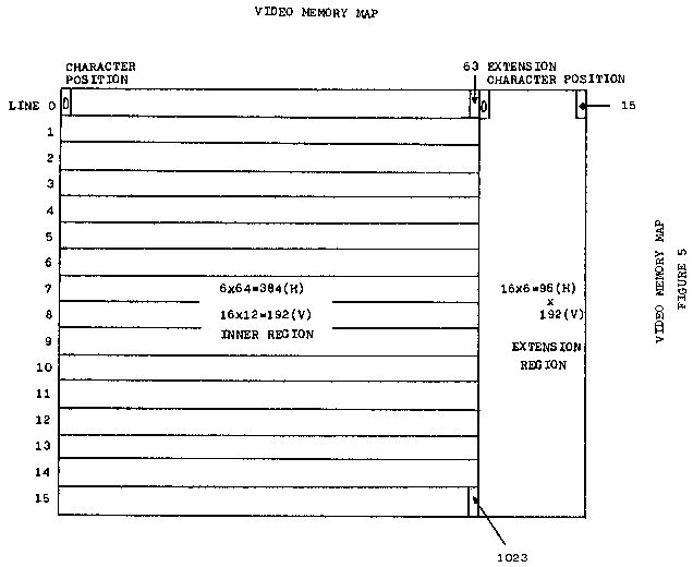
For the following discussion refer to figure 5, the
VIDEO MEMORY MAP. Note that the low resolution video is
defined only within the inner region and that A10-A13, which
specify the row count are not used by the low resolution video
ram. By definition A10-A13 are at a logic "1" voltage state
during CPU access of the low resolution video ram.
The inner region represents the standard TRS80* video
display. This region is memory mapped at locations 15360
through 16383. It has 63 characters and 16 lines, each line
with 12 rows. The video addressing of this region is
represented by the following:
were in 64 character mode. T5* is selected as CNTRCLK and
CHAR1 is ground. Note that because T7* is 1/2 the frequency
of T5*, by selecting T5* in 32 character mode CNTRCLK does not
change and therefore nor does the resulting logic of U160 and
U161.
The signals that did change, T2 through T5 and CHAR1,
are very important to the video processor section. CHAR1
determines whether the video ram have 1024 or512 usable
addresses. T2 through T5 determine how many characters may be
processed to the character generator per line.
VIDEO RAM ADDRESSING
The video rams are addressed by 2 sources. The video
divider chain addresses the video ram so that data contained
in memory can be processed and displayed on the screen. The
CPU must address the video ram so that data can be read from
or writen to specific locations. Multiplexers are used to
select either the video chain or CPU address.
For the following discussion refer to figure 5, the
VIDEO MEMORY MAP. Note that the low resolution video is
defined only within the inner region and that A10-A13, which
specify the row count are not used by the low resolution video
ram. By definition A10-A13 are at a logic "1" voltage state
during CPU access of the low resolution video ram.
The inner region represents the standard TRS80* video
display. This region is memory mapped at locations 15360
through 16383. It has 63 characters and 16 lines, each line
with 12 rows. The video addressing of this region is
represented by the following:
 AO-A5 specify character position 0-63, A6-A9 specify
line position 0-15, and A10-A13 specify row position 0-11.
A14 and A15 will be low.
The extension region, refer to figure 5, adds an
additional 16 character positions for a total of 80. The
following illustrates the addressing of this region:
AO-A5 specify character position 0-63, A6-A9 specify
line position 0-15, and A10-A13 specify row position 0-11.
A14 and A15 will be low.
The extension region, refer to figure 5, adds an
additional 16 character positions for a total of 80. The
following illustrates the addressing of this region:
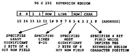 A0-A3 specify character 0-15 of the extension
region, A4-A5 specify the most significant 2 bits of the 4
bit row field, A6-A9 specify lines 0-15, and A10-A11 specify
the least significant 2 bits of the 4 bit row field. A12
and A13 are high. Note that the extension region is
uniquely defined by a logic"1" at A12 and A13 because in the
inner region this would specify a row count greater than
11.
When the CPU is not accessing the video ram, the
video addresses are controlled by the video divider chain.
The selects at U139, U148, 0144, and u145 will be high
selecting the B inputs.
U142 specifies whether we are in the inner or
extension region. Prior to the 64th character HORTP(U142-1)
will be low, selecting the A inputs. At the 64th character
HORTP will go high selecting the B inputs thus selecting the
extension region addresses.
CPUACC*(U121-8) is the select for U139, U148, U144,
and U145. When the CPU is accessing the video ram, CPUACC+
will go low selecting the A inputs. The procedure by which
CPUACC* goes low and the CPU addresses are latched into the
address multiplexers will be covered in a following
section.
LOW RESOLUTION VIDEO RAM
The Low-Resolution Video Ram consists of two 2114
type 1Kx4 static ram chips. For either read or write
operations the select (pin 8) must be low. They have an
active low write enable, 10 address lines, and 4 data lines
each. U114 uses the least 4 significant data bits and U115
the 4 most significant data bits.
When the CPU wishes to access the video ram it
must execute a read or write operation while placing a video
address on the address bus. For the Low-Resolution (LORES)
Video Ram this address must be from (3C00-3FFF)Hex. The
following illustrates the sequence of events during a LORES
video write.
During the execution of a LORES video write, the CPU
will place a video address on the address bus. This address
will be decoded at U6 and U35 resulting with a logic "0" at
VID*(U35-7). WR* will be low. These are the inputs to U152
pins 4 and 5 respectively. When both are low the output,
VIDWRT*(U152-6), will go low. This is the input to U154, a
four input nand gate. Note that the four inputs represent
LORES video write, LORES video read, HIRES video write, and
HIRES video read. When any of the four inputs goes low the
output, pin6 will go high clocking U153. DATALAT(U153-5)
will be high and U153-6 will be low. CLKADRSDTA (U137-6)
will go high latching U98, U141, and U143. Thus the CPU
addresses, the CPU data, and VIDWRT* are latched. VIDWRT*
is latched at U141-4. It becomes LVIDWRT*. LVIDWRT* and
T2* are input at U151 pins 12 and 13 respectively. T2*
prevents the LORES video ram to be written to before the
video addresses are stabilized. At the beginning of the
next video timing cycle Tl will clock DATALAT into U121
resulting in a logic "0" at CPUACC*(U121-8). CPUACC* is the
select of the video address multiplexers and when it is low
the CPU addresses are selected. At T2*, LVIDWRT* will be
output to WRT2114* (U139-12). WRT2I14* enables the data
output of U98 through U81 and is the write enable to the
LORES rams. The write operation is completed when T6*
clears U153, and the resuIting 1ow signal at DATALAT clears
U121. CPUACC* goes high and the video address is returned
to the video divider chain.
A LORES video, read is very similar to the write.
VID* will be decoded from the video address. RD* will be
low. These are the inputs to U152 pins 1 and 2
respectively. This will place a low input to U154 as before
and the same signals will result except VIDWRT* will be high
and VIDRD* will be low. At the end of the operation DATALAT
will go low latching in data at U99 and U125. VIDRD*
enables the output of U99 from which the CPU will read the
data.
HI RESOLUTION GRAPHICS RAM
The Hi Resolution (HIRES) Graphics Ram are located
at the lower 16K of the LNW80 address space. Note that this
is also where the Roms, keyboard, LORES video ram, and
miscellaneous I/0 are mapped. I/0 port 254 bit-D3 selects
which devices are enabled. With D3=1, the graphics memory
is enabled. Note that since the Roms are also disabled by
D3=1, using the OUT command in basic to turn on this bit
will be fatal to the computer since the computer will
execute out of graphics Ram instead of Rom.
A0-A3 specify character 0-15 of the extension
region, A4-A5 specify the most significant 2 bits of the 4
bit row field, A6-A9 specify lines 0-15, and A10-A11 specify
the least significant 2 bits of the 4 bit row field. A12
and A13 are high. Note that the extension region is
uniquely defined by a logic"1" at A12 and A13 because in the
inner region this would specify a row count greater than
11.
When the CPU is not accessing the video ram, the
video addresses are controlled by the video divider chain.
The selects at U139, U148, 0144, and u145 will be high
selecting the B inputs.
U142 specifies whether we are in the inner or
extension region. Prior to the 64th character HORTP(U142-1)
will be low, selecting the A inputs. At the 64th character
HORTP will go high selecting the B inputs thus selecting the
extension region addresses.
CPUACC*(U121-8) is the select for U139, U148, U144,
and U145. When the CPU is accessing the video ram, CPUACC+
will go low selecting the A inputs. The procedure by which
CPUACC* goes low and the CPU addresses are latched into the
address multiplexers will be covered in a following
section.
LOW RESOLUTION VIDEO RAM
The Low-Resolution Video Ram consists of two 2114
type 1Kx4 static ram chips. For either read or write
operations the select (pin 8) must be low. They have an
active low write enable, 10 address lines, and 4 data lines
each. U114 uses the least 4 significant data bits and U115
the 4 most significant data bits.
When the CPU wishes to access the video ram it
must execute a read or write operation while placing a video
address on the address bus. For the Low-Resolution (LORES)
Video Ram this address must be from (3C00-3FFF)Hex. The
following illustrates the sequence of events during a LORES
video write.
During the execution of a LORES video write, the CPU
will place a video address on the address bus. This address
will be decoded at U6 and U35 resulting with a logic "0" at
VID*(U35-7). WR* will be low. These are the inputs to U152
pins 4 and 5 respectively. When both are low the output,
VIDWRT*(U152-6), will go low. This is the input to U154, a
four input nand gate. Note that the four inputs represent
LORES video write, LORES video read, HIRES video write, and
HIRES video read. When any of the four inputs goes low the
output, pin6 will go high clocking U153. DATALAT(U153-5)
will be high and U153-6 will be low. CLKADRSDTA (U137-6)
will go high latching U98, U141, and U143. Thus the CPU
addresses, the CPU data, and VIDWRT* are latched. VIDWRT*
is latched at U141-4. It becomes LVIDWRT*. LVIDWRT* and
T2* are input at U151 pins 12 and 13 respectively. T2*
prevents the LORES video ram to be written to before the
video addresses are stabilized. At the beginning of the
next video timing cycle Tl will clock DATALAT into U121
resulting in a logic "0" at CPUACC*(U121-8). CPUACC* is the
select of the video address multiplexers and when it is low
the CPU addresses are selected. At T2*, LVIDWRT* will be
output to WRT2114* (U139-12). WRT2I14* enables the data
output of U98 through U81 and is the write enable to the
LORES rams. The write operation is completed when T6*
clears U153, and the resuIting 1ow signal at DATALAT clears
U121. CPUACC* goes high and the video address is returned
to the video divider chain.
A LORES video, read is very similar to the write.
VID* will be decoded from the video address. RD* will be
low. These are the inputs to U152 pins 1 and 2
respectively. This will place a low input to U154 as before
and the same signals will result except VIDWRT* will be high
and VIDRD* will be low. At the end of the operation DATALAT
will go low latching in data at U99 and U125. VIDRD*
enables the output of U99 from which the CPU will read the
data.
HI RESOLUTION GRAPHICS RAM
The Hi Resolution (HIRES) Graphics Ram are located
at the lower 16K of the LNW80 address space. Note that this
is also where the Roms, keyboard, LORES video ram, and
miscellaneous I/0 are mapped. I/0 port 254 bit-D3 selects
which devices are enabled. With D3=1, the graphics memory
is enabled. Note that since the Roms are also disabled by
D3=1, using the OUT command in basic to turn on this bit
will be fatal to the computer since the computer will
execute out of graphics Ram instead of Rom.
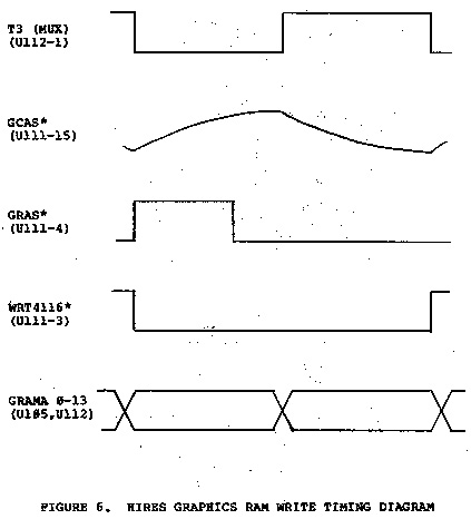 The HIRES Ram utilizes six, 16Kx1 dynamic memories.
The addressing sequence of events is GRAS*(row address
select), T3(multiplex), then GCAS*(column address select) to
multiplex the 14 bits of address into 7-bit parts. The
sequence of events during a write operation are as follows.
I/0 Port 254 is decoded by U33 and U54. FEOUT*
(U54-12) is used to clock U67. When U67 is clocked and
D3=1, GRRDEN* (U67-6) becomes logic "0". This inputs to
U66-12. When the CPU places an address of the lower 16K on
the address bus, A14 and A15 will be low at U66 pins 10 and
9 respectively. This is used to decode the lower 16K. The
output of U66-8 goes low and inputs to U66-13. This enables
GLWR16K* at U66-11. GLWR16K* is inverted at U51 and becomes
RDWRDIS (read write disable). RDWRDIS disables
RDOUT*(U36-8) and WROUT*(U36-11) preventing a conflict on
the data bus. GLWR16K* is input to U152 pins 9 and 12.
When accompanied with either IRD* or IWR* a read or write
operation will occur at the HIRES Ram. Suppose that IWR*
(U152-18) goes low. Then GRAMWRT* (U152-8) will enable
U154-4. The video address and data control signals are the
same as far the LORES write operation. WRT4116* (U139-4) is
inverted through U118 to disable the LORES Ram. Figure 6
illustrates the timing diagram during a write operation.
The read operation is very similar except that
GRAMWRT* remains high and GRAMEN* goes low enabling U154.
Refer to the write operation for complete details of the
address latching and multiplexing. The data is latched into
U125 from pin 14 of the HRES Ram by DATALAT, and the outputs
of U125 are enabled by GRAMEN*. The CPU reads the data from
U125. Note that D6 and D7 have inputs HORTP and VERTTP. In
the present usage these bits are not used.
VIDEO DATA LATCH
The first step of the video processing is the data
latch. For the LORES video this occurs at U116 and U117
(LS174's). U116 latches the lower 5 data bits. U117
latches D6 and D7, also the video control signals. D0-D5
and D7 are latched directly at the end of the timing chain
cycle by T5*. D6 passes through U81 and U82. When CAPS*
(U82-4) is true D6 is disabled, and DLYD6 becomes a function
of D5 and D7. The purpose of the CAPS* key is to disable
lower case characters. The ASCII code for lower case is
within (68-7F)Hex. D6 is a "1" for all lower case
characters. When a lower case character is decoded and the
CAPS* key is depressed, DLYD6 will be "0" thus disabling
lower case. The HIRES video also uses an LS174, U126, and
it too is clocked by T5*.
CHARACTER GENERATOR
Each character consists of a 5x7 dot matrix.
Between any two characters there is a dot that is never
turned on. Vertical spacing between dots is determined by
CLKT. Note that in 32 character mode CLKT is 1/2 the 64
character mode CLKT frequency. This means that in 32
character mode there will be twice the vertical spacing
between dots.
U100 is the Character Generator. The ASCII word is
presented to U100 pins 1 through 7 from U116 and U117. U188
uses the ROW count to determine which patern of five dots to
print on each row. It must output 7 times to complete one
character after which five rows of blanks are output and the
line increments and we're ready to output the first row of
dot information to the 2nd character line.
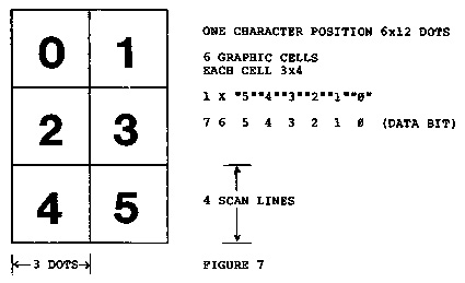
GRAPHICS GENERATOR
U83 functions as the Graphics (LORES) Generator.
The Graphics Character may use the entire character
position, a 6x12 dot matrix. This matrix is divided into
six rectangles as shown in figure 7. U83 is a dual 4x1 data
multiplexer. It uses ROW4 and ROW8 as selects. Each 3x4
rectangle is either "on" of "off'. When the ROW count is
between 0 and 3, DLYDB AND DLYD1 are selected. When the ROW
count is between 3 and 7, DLYD2 and DLYD3 are selected. And
finally for a ROW count between 8 and 11, DLYD4 and DLYD5
are selected. Each scan line, 3 dots may be written in each
of two rectangles per graphic character. Each rectangle is
defined by one data bit. DLYD7 defines a graphics character
when true.
The HIRES Ram utilizes six, 16Kx1 dynamic memories.
The addressing sequence of events is GRAS*(row address
select), T3(multiplex), then GCAS*(column address select) to
multiplex the 14 bits of address into 7-bit parts. The
sequence of events during a write operation are as follows.
I/0 Port 254 is decoded by U33 and U54. FEOUT*
(U54-12) is used to clock U67. When U67 is clocked and
D3=1, GRRDEN* (U67-6) becomes logic "0". This inputs to
U66-12. When the CPU places an address of the lower 16K on
the address bus, A14 and A15 will be low at U66 pins 10 and
9 respectively. This is used to decode the lower 16K. The
output of U66-8 goes low and inputs to U66-13. This enables
GLWR16K* at U66-11. GLWR16K* is inverted at U51 and becomes
RDWRDIS (read write disable). RDWRDIS disables
RDOUT*(U36-8) and WROUT*(U36-11) preventing a conflict on
the data bus. GLWR16K* is input to U152 pins 9 and 12.
When accompanied with either IRD* or IWR* a read or write
operation will occur at the HIRES Ram. Suppose that IWR*
(U152-18) goes low. Then GRAMWRT* (U152-8) will enable
U154-4. The video address and data control signals are the
same as far the LORES write operation. WRT4116* (U139-4) is
inverted through U118 to disable the LORES Ram. Figure 6
illustrates the timing diagram during a write operation.
The read operation is very similar except that
GRAMWRT* remains high and GRAMEN* goes low enabling U154.
Refer to the write operation for complete details of the
address latching and multiplexing. The data is latched into
U125 from pin 14 of the HRES Ram by DATALAT, and the outputs
of U125 are enabled by GRAMEN*. The CPU reads the data from
U125. Note that D6 and D7 have inputs HORTP and VERTTP. In
the present usage these bits are not used.
VIDEO DATA LATCH
The first step of the video processing is the data
latch. For the LORES video this occurs at U116 and U117
(LS174's). U116 latches the lower 5 data bits. U117
latches D6 and D7, also the video control signals. D0-D5
and D7 are latched directly at the end of the timing chain
cycle by T5*. D6 passes through U81 and U82. When CAPS*
(U82-4) is true D6 is disabled, and DLYD6 becomes a function
of D5 and D7. The purpose of the CAPS* key is to disable
lower case characters. The ASCII code for lower case is
within (68-7F)Hex. D6 is a "1" for all lower case
characters. When a lower case character is decoded and the
CAPS* key is depressed, DLYD6 will be "0" thus disabling
lower case. The HIRES video also uses an LS174, U126, and
it too is clocked by T5*.
CHARACTER GENERATOR
Each character consists of a 5x7 dot matrix.
Between any two characters there is a dot that is never
turned on. Vertical spacing between dots is determined by
CLKT. Note that in 32 character mode CLKT is 1/2 the 64
character mode CLKT frequency. This means that in 32
character mode there will be twice the vertical spacing
between dots.
U100 is the Character Generator. The ASCII word is
presented to U100 pins 1 through 7 from U116 and U117. U188
uses the ROW count to determine which patern of five dots to
print on each row. It must output 7 times to complete one
character after which five rows of blanks are output and the
line increments and we're ready to output the first row of
dot information to the 2nd character line.
GRAPHICS GENERATOR
U83 functions as the Graphics (LORES) Generator.
The Graphics Character may use the entire character
position, a 6x12 dot matrix. This matrix is divided into
six rectangles as shown in figure 7. U83 is a dual 4x1 data
multiplexer. It uses ROW4 and ROW8 as selects. Each 3x4
rectangle is either "on" of "off'. When the ROW count is
between 0 and 3, DLYDB AND DLYD1 are selected. When the ROW
count is between 3 and 7, DLYD2 and DLYD3 are selected. And
finally for a ROW count between 8 and 11, DLYD4 and DLYD5
are selected. Each scan line, 3 dots may be written in each
of two rectangles per graphic character. Each rectangle is
defined by one data bit. DLYD7 defines a graphics character
when true.
 ALPHANUMERIC/GRAPHIC SHIFT REGISTERS
U101 is the alphanumeric shift register, U84 is the
LORES graphic shift register, and U127 is the HIRES graphic
shift register. All three receive parallel data and shift
that data out to the video display in serial form.
All three behave in the same manner but have
different restrictions that if not met will prevent data
from being serialized.
The inputs to U102 pins 1,2,4, and 5 represent the
restrictions to the alphanumeric shift register. If any of
the inputs go low, the output will go high thus preventing
the loading of data. DLYROW8* provides the blanking of ROWs
8 through 11 for alphanumeric characters. DLYBLANK*
provides blanking beyond the 64th character position and
below the 16th line. DLYD7* defines an alpha numeric
character when true. And CTRLT5(U81-8) provides that data
in not loaded during CPU access time. Nate that there are
only 5 inputs to U181. This is because the sixth bit is
tied to gnd to blank the sixth dot between characters.
The inputs to U85 pins 1,2, and 13 represent the
restrictions to the LORES graphics shift register. If any
of its inputs go low its output will go high preventing data
from being loaded. There are two differences in the
restrictions of the LORES graphics and the alphanumeric
shift registers. The first is that for graphics characters
the entire character position may be used therefore ROWs 8
through 11 are not blanked out. And DLYD7 defines a
qraphics character when true. The restriction regarding
CTRLT5 still applies.
The inputs to U85 pins 3,4, and 5 represent the
restrictions to the HIRES graphics shift register. CTRLT5
has the same purpose as described far the alphanumeric shift
register. DLYLDHDG* provides blanking after the 80th
character and below the 16th line. DLYLDINH* prevents
loading during CPU access time.
INVERSE VIDEO
Inverse Video is controlled through Port 254. When
D0 is set to a one and output to Port 254, VIDEOINV (U67-18)
becomes a logic one. VIDEOINV drives U82-1 an input of an
exclusive or gate (74LS86). When VIDEOINV is a "1" the
combined video output of U68-4 (VIDEO "NORed" with HRESVID)
is complemented thus inverting the video content. This is
full screen video. When VIDEOINV is low the combined video
information passes unchanged (standard video). The output
of U82-3 COMBINED VIDEO (COMBVID*) drives both the high
resolution B/W video output circuitry (U9-6,7) and the NTSC
color channel (in the non-color display modes) at U68-11.
HORIZONTAL AND VERTICAL SYNC TIMING
U20 and U37 form the sync generator circuit. The
horizontal and vertical sync generator circuits take the
timing pulses from the divider chain, delays are applied to
them, and the pulses are one-shot to fix the pulse width.
This allows the vertical and horizontal positions to be
adjustable and the correct pulse width is supplied to the
video monitor to provide the correct horizontal and vertical
synchronization.
The VERTICAL TIMING PULSE (VERTTP) from the divider
chain is buffered by U20-8 (a CMOS exclusive or acting as a
buffer only) and drives potentiometer R145. When R145 is
set for some resistance U20-10 directly drives an RC timing
delay circuit formed by R145 and C23. When VERTTP goes to a
logic "1", C23 begins to charge. As it charges, the voltage
at the input of U37-5 (74C04) rises. When the voltage
reaches the threshold of a 1ogic "1" (around 4 volts since
this is CHMOS 1ogic), the output of U37-6 becomes a logic 0
(U37 is an inverter). The logic 0 output of U37-6 drives
the input of the next inversion stage of U37-9. The 1ogic 0
is inverted and the output of U37-8 becomes a logic "1" and
stays that way until VERTTP returns to a logic "0". By
changing the "R" af the R145 and C23 "RC" circuit the
vertical sync pulse is varied. This allows the adjustable
vertical screen position to compensate for variance in video
monitors. The output of U37-8 is now given a fixed pulse
width by the monostable circuitry of C22, R49 and the input
of U37-1.
The horizontal sync circuits work in a similar manner
with the HORIZONTAL SYNC TINING PULSE (HSTP) driving U20-13.
R144 and C24 form the RC delay, and C21 and R48 farm the
pulse shaping and width.
The horizontal and vertical sync pulses are mixed by
two EXCLUSIVE OR gates of U20. The output of U20-3 directly
drives the video mixing circuits of the Hi-resolution B/W
video output. U20-4 drives the Sync input to the NTSC
Prom.
U118-9,8 buffers the horizontal sync circuits to
signal the Burst one-shot (U133-1) of the horzontal sync
period. The Burst one-shot is described further in the
section entitled "COLOR VIDEO".
COMPOSITE VIDEO MIXING CIRCUITS (HI-RES)
The following drawing illustates what the black and
white video output would look like with an oscilloscope.
ALPHANUMERIC/GRAPHIC SHIFT REGISTERS
U101 is the alphanumeric shift register, U84 is the
LORES graphic shift register, and U127 is the HIRES graphic
shift register. All three receive parallel data and shift
that data out to the video display in serial form.
All three behave in the same manner but have
different restrictions that if not met will prevent data
from being serialized.
The inputs to U102 pins 1,2,4, and 5 represent the
restrictions to the alphanumeric shift register. If any of
the inputs go low, the output will go high thus preventing
the loading of data. DLYROW8* provides the blanking of ROWs
8 through 11 for alphanumeric characters. DLYBLANK*
provides blanking beyond the 64th character position and
below the 16th line. DLYD7* defines an alpha numeric
character when true. And CTRLT5(U81-8) provides that data
in not loaded during CPU access time. Nate that there are
only 5 inputs to U181. This is because the sixth bit is
tied to gnd to blank the sixth dot between characters.
The inputs to U85 pins 1,2, and 13 represent the
restrictions to the LORES graphics shift register. If any
of its inputs go low its output will go high preventing data
from being loaded. There are two differences in the
restrictions of the LORES graphics and the alphanumeric
shift registers. The first is that for graphics characters
the entire character position may be used therefore ROWs 8
through 11 are not blanked out. And DLYD7 defines a
qraphics character when true. The restriction regarding
CTRLT5 still applies.
The inputs to U85 pins 3,4, and 5 represent the
restrictions to the HIRES graphics shift register. CTRLT5
has the same purpose as described far the alphanumeric shift
register. DLYLDHDG* provides blanking after the 80th
character and below the 16th line. DLYLDINH* prevents
loading during CPU access time.
INVERSE VIDEO
Inverse Video is controlled through Port 254. When
D0 is set to a one and output to Port 254, VIDEOINV (U67-18)
becomes a logic one. VIDEOINV drives U82-1 an input of an
exclusive or gate (74LS86). When VIDEOINV is a "1" the
combined video output of U68-4 (VIDEO "NORed" with HRESVID)
is complemented thus inverting the video content. This is
full screen video. When VIDEOINV is low the combined video
information passes unchanged (standard video). The output
of U82-3 COMBINED VIDEO (COMBVID*) drives both the high
resolution B/W video output circuitry (U9-6,7) and the NTSC
color channel (in the non-color display modes) at U68-11.
HORIZONTAL AND VERTICAL SYNC TIMING
U20 and U37 form the sync generator circuit. The
horizontal and vertical sync generator circuits take the
timing pulses from the divider chain, delays are applied to
them, and the pulses are one-shot to fix the pulse width.
This allows the vertical and horizontal positions to be
adjustable and the correct pulse width is supplied to the
video monitor to provide the correct horizontal and vertical
synchronization.
The VERTICAL TIMING PULSE (VERTTP) from the divider
chain is buffered by U20-8 (a CMOS exclusive or acting as a
buffer only) and drives potentiometer R145. When R145 is
set for some resistance U20-10 directly drives an RC timing
delay circuit formed by R145 and C23. When VERTTP goes to a
logic "1", C23 begins to charge. As it charges, the voltage
at the input of U37-5 (74C04) rises. When the voltage
reaches the threshold of a 1ogic "1" (around 4 volts since
this is CHMOS 1ogic), the output of U37-6 becomes a logic 0
(U37 is an inverter). The logic 0 output of U37-6 drives
the input of the next inversion stage of U37-9. The 1ogic 0
is inverted and the output of U37-8 becomes a logic "1" and
stays that way until VERTTP returns to a logic "0". By
changing the "R" af the R145 and C23 "RC" circuit the
vertical sync pulse is varied. This allows the adjustable
vertical screen position to compensate for variance in video
monitors. The output of U37-8 is now given a fixed pulse
width by the monostable circuitry of C22, R49 and the input
of U37-1.
The horizontal sync circuits work in a similar manner
with the HORIZONTAL SYNC TINING PULSE (HSTP) driving U20-13.
R144 and C24 form the RC delay, and C21 and R48 farm the
pulse shaping and width.
The horizontal and vertical sync pulses are mixed by
two EXCLUSIVE OR gates of U20. The output of U20-3 directly
drives the video mixing circuits of the Hi-resolution B/W
video output. U20-4 drives the Sync input to the NTSC
Prom.
U118-9,8 buffers the horizontal sync circuits to
signal the Burst one-shot (U133-1) of the horzontal sync
period. The Burst one-shot is described further in the
section entitled "COLOR VIDEO".
COMPOSITE VIDEO MIXING CIRCUITS (HI-RES)
The following drawing illustates what the black and
white video output would look like with an oscilloscope.
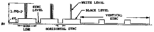 The "sync level" extends from 0 volts to .4 volts.
This .4 volt level is commonly referred to as the "black
level" no the voltage that would leave the display black.
Above 1.2 volts is the white level. Between these levels
are shades of gray. When a pixel is displayed an the CRT,
the voltage goes above 1.2 volts for just enough time to
display the dot. If most of the screen is blanked, looking
at the video signal with an oscilloscope should show few
very thin pulses extending to 1.2 volts with most of the
time the voltage staying below .4 volts.
The combined sync output of U20-3 directly drives the
base of Q2. When there is sync, U20-3 is high and Q2 is
turned off. This provides no drive to Q1 and thus the video
output is 0 volts. During the non-sync period U20-3 is
"low" and "turns on" Q2. This causes 5 volts to be driven
into voltage divider R19 and R16 and the base of Q1. The
COMBINED VIDEO output (COMBVID*) drives peripheral and
driver U9. When the video dot is to be displayed
(COMBVID*=0) then the output transistor in U9 is "off" thus
high impedance. This means that R17 has no effect in the
circuit and around 2.5 volts drives the base of
emitter-follower Q1. With around .7 volts drop the output
of Q1 (75 ohms impedance) is 1.8 volts. When the video dot
is NOT to be displayed, COMBVID* is high and R17 now appears
in the circuit from the base of Q1 to ground. This causes
the voltage at the base of Q1 to be reduced to around 1 volt
thus with a .7 volt drop at Q1 (base to emitter) the output
is at the "black level" or .4 volts. C7, R22, and C8 serve
to filter, reduce power dissipation in Q1, and serve as
short-circuit protection. R121 serves to set the output
impedance of the video signal.
NTSC COLOR VIDEO
NTSC stands for the television standard first,
developed and implemented in the United States. Japan,
Canada, and Mexico also adopted this (the first) television
standard. NTSC color video uses the same timing and levels
as Black and White video. It has a 60 hz vertical sync rate
which corresponds to 262 scanned lines (including sync).
The LNW80 refreshes the screen at a rate of 60 hz with 262
lines. Countries which have AC power frequencies of 50hz use
PAL, SECAM, or other color systems with 312 scanned lines at
a 50hz vertical rate. These systems are not compatible with
the LNW80 set up for NTSC at 60hz.
Color video works much the same as black and white.
The video signal also is 1.8v p-p and .4 v is the black
level and 1.2v is the white level. Horizontal and vertical
sync are identical. Here are the differences:
1. COLOR ENCODING
In order to encode color information on the video
signal there is a COLOR CARRIER. This color carrier allows
the luminance information to be encoded with a PHASE
relationship with the carrier thus specifying the color to
be displayed.
2. COLOR BURST
The color carrier cannot be present during the displayed
video period and thus is maintained by the monitor (or TV).
This 3.579545 MHz signal is transmitted only far a small
period of time by the computer (or TV station) to keep the
color oscillator in the monitor (or TV) "locked in at the
same exact frequency". This "burst" of color carrier is
transmitted only for about 8 cycles and only at the very end
of the horizontal sync pulse. This is commonly referred to
as the "back porch" of the horizontal sync or the COLOR
BURST and is illustated below:
The "sync level" extends from 0 volts to .4 volts.
This .4 volt level is commonly referred to as the "black
level" no the voltage that would leave the display black.
Above 1.2 volts is the white level. Between these levels
are shades of gray. When a pixel is displayed an the CRT,
the voltage goes above 1.2 volts for just enough time to
display the dot. If most of the screen is blanked, looking
at the video signal with an oscilloscope should show few
very thin pulses extending to 1.2 volts with most of the
time the voltage staying below .4 volts.
The combined sync output of U20-3 directly drives the
base of Q2. When there is sync, U20-3 is high and Q2 is
turned off. This provides no drive to Q1 and thus the video
output is 0 volts. During the non-sync period U20-3 is
"low" and "turns on" Q2. This causes 5 volts to be driven
into voltage divider R19 and R16 and the base of Q1. The
COMBINED VIDEO output (COMBVID*) drives peripheral and
driver U9. When the video dot is to be displayed
(COMBVID*=0) then the output transistor in U9 is "off" thus
high impedance. This means that R17 has no effect in the
circuit and around 2.5 volts drives the base of
emitter-follower Q1. With around .7 volts drop the output
of Q1 (75 ohms impedance) is 1.8 volts. When the video dot
is NOT to be displayed, COMBVID* is high and R17 now appears
in the circuit from the base of Q1 to ground. This causes
the voltage at the base of Q1 to be reduced to around 1 volt
thus with a .7 volt drop at Q1 (base to emitter) the output
is at the "black level" or .4 volts. C7, R22, and C8 serve
to filter, reduce power dissipation in Q1, and serve as
short-circuit protection. R121 serves to set the output
impedance of the video signal.
NTSC COLOR VIDEO
NTSC stands for the television standard first,
developed and implemented in the United States. Japan,
Canada, and Mexico also adopted this (the first) television
standard. NTSC color video uses the same timing and levels
as Black and White video. It has a 60 hz vertical sync rate
which corresponds to 262 scanned lines (including sync).
The LNW80 refreshes the screen at a rate of 60 hz with 262
lines. Countries which have AC power frequencies of 50hz use
PAL, SECAM, or other color systems with 312 scanned lines at
a 50hz vertical rate. These systems are not compatible with
the LNW80 set up for NTSC at 60hz.
Color video works much the same as black and white.
The video signal also is 1.8v p-p and .4 v is the black
level and 1.2v is the white level. Horizontal and vertical
sync are identical. Here are the differences:
1. COLOR ENCODING
In order to encode color information on the video
signal there is a COLOR CARRIER. This color carrier allows
the luminance information to be encoded with a PHASE
relationship with the carrier thus specifying the color to
be displayed.
2. COLOR BURST
The color carrier cannot be present during the displayed
video period and thus is maintained by the monitor (or TV).
This 3.579545 MHz signal is transmitted only far a small
period of time by the computer (or TV station) to keep the
color oscillator in the monitor (or TV) "locked in at the
same exact frequency". This "burst" of color carrier is
transmitted only for about 8 cycles and only at the very end
of the horizontal sync pulse. This is commonly referred to
as the "back porch" of the horizontal sync or the COLOR
BURST and is illustated below:
 COLOR MODES
In the LNW80 there are two possible color modes-1ow
resolution and high resolution. The bandwidth of NTSC video
only allows the low resolution mode to be displayed. In
order to display the high resolution color, an RGB type
direct drive monitor must be used and the optional RGB
interface circuitry must be installed.
Port 254 data bit 2 selects whether or not color is
enabled. COLOR (U67-2) and COLOR* (U67-3) do the logic
switching to enable or disable color operation.
LOW RESOLUTION COLOR
In low resolution color mode, HRES will be low and
HRES* will be high. This causes U129 to be enabled and U131
to be disabled via two .gates of U52. U52-13 (COLOR) is
high, U52-2 (HRES+) is high and U52-1 is VIDEO, thus the
output of U52-12 which allows U129 to be selected to drive
color information to U130 (NTSC ROM) will go low along with
VIDEO. This means that the law resolution text and graphics
information from the MODE 0 display will select whether or
not the color information is to be passed on the NTSC ROM or
the display will be black. When U129 is not enabled (it is a
tri-state) gate pull-up resistors R101, R100, and R93 pull
the floating inputs of the NTSC ROM to a logic "1". A logic
"1" on all three bits of the color code or a 7 is defined as
the color black. This means that there are two ways that
the screen can be programmed black. One by putting 7 as the
color information in the color memory or by blanking the low
res screen.
Color information is stored in the same memory as the
high resolution graphics memory U186-U111. The 6 bits of
data, instead of being fed into a shift register (U127) to
be sent out one bit at a time (as in high resolution
graphics), is latched again into U128. It is fed to U128
for another level of delay to syncronize the Black and White
video information (being shifted out of U101 or U84). Once
latched into U128, the 6 bits represent two 3 bit (1 of 7
colors and black) fields. During the period that the first
3 dots (of the character position time) are being shifted
out of U84 or U101, T3 is a logic 0. This drives the least
significant 3 bits of U128 into the NTSC ROM to define the
color. During the next 3 dot periods, T3 is a logic 1 and
the most significant 3 bits of U128 are driven into U138 to
define the color. Remember that if VIDEO was false, U129 is
disabled completely thus overriding the contents of U128
(displaying black).
NTSC COLOR ROM
The NTSC COLOR ROM translates a 3 bit color code
(0-7), SYNC and BURST (timing) inta the proper A-Y (COLORB),
B-Y (COLORA), and LUMINANCE (LUM) that the MC1372 requires
to do the color encoding. The NTSC ROM (U138) is a high
speed bipolar open collector prom. U138 combined with
ladder resistors R85-92, R94, R99 and R102-185 form a high
speed digital to analog converter to translate the digital
color codes and sync information into the analog levels
needed by the NC1372.
The following is the truth table for the NTSC ROM
and the voltage levels developed for COLORA, COLORB, and
LUM.
ADDRESS DATA(Hex) COLORA COLOAB LUM
(Hex) COLOR SYNC BURST
A0 Al A2 A3 A4 COLOR
===========================================================
00 0 0 0 0 0 6C WHITE 1.5V 1.5V .38
01 1 0 0 0 0 D5 GREEN 1.0 1.0 .5
02 0 1 0 0 0 CC YELLOW 1.5 1.0 .38
03 1 1 0 0 0 7A RED 2.0 1.5 .62
04 0 0 1 0 0 FD MAGENTA 2.0 2.0 .50
05 1 0 1 0 0 EA BLUE 1.5 2.0 .62
06 8 1 1 0 0 75 CYAN 1.0 1.5 .50
07 1 1 1 0 0 6B BLACK 1.5 1.5 .78
08 0 0 0 1 0 6F SYNC 1.5 l.5 1.00
======================== to
0F 1 1 1 1 0 6P SYNC 1.5 1.5 1.00
10 0 00 0 0 1 AE BURST 1.5 1.25 .75
======================== to
17 1 1 1 0 1 AE BURST 1.5 1.25 .75
18 0 0 0 1 1 6F SYNC 1.5 1.5 1.00
======================== to
1F 1 1 1 1 1 6F SYNC 1.5 1.5 1.00
COLOR BURST ONE-SHOT
When HSYNC transitions from high to 1ow (the end of
the horizontal sync pulse) U133-13 strobes, using R80 and
C83 for RC timing. The one-shot time is approximately
2usec. During this time, BURST is high and drives A4 of
U130, the NTSC ROM. When A4 is high, the correct analog
levels are supplied to U146 (NC1372) to output a burst
reference signal with the correct phase and amplitude.
U146-MC1372 COLOR ENCODER
The MC1372 is a linear IC which contains both a
chroma oscillator and the necessary chroma (color) encoder.
U146 pins 1 and 2 along with Y2 the 3.579545 MHz crystal,
C94 and 95, and R106 form the complete color reference
oscillator (chroma oscillator) circuit. C95 is the chroma
frequency trimmer adjustment. U146-1 is the square wave
output of the 3.579 MHz color frequency and drives one-shot
U133-10 to provide the color to luminance dot clock
synchronization signal (COLORSYNC). U133 with timing
resistor R187 (and no timing capacitor) forms a 50-70
nanosecond pulse generator. U133-5 drives open-collector
inverter U162-11. Inverted and pulled up by R97, this
generates COLORSYNC.
COLORA, COLORB, and LUN information from U130
determines the luminance level and the phase encoding of the
video information that is output by the NC1372 on pin 12.
R109 sets the output bias and CR1 selects the composite
video polarity. The output of U146-12 (COLOROUT) is
amplified and level shifted by Q13, R123 and R129. Q14 is
an emitter follower to provide current amplification and 75
ohm impedance matching.
The MC1372 has the chroma encoder circuit separate
from the final composite video mixing circuit. The chroma
encoder output (U146-10) is fed back into U146-8 through
A117 and blocking capacitor C110. UI62-12, Clll, and R118
form the chroma killer circuit that disables any chroma
content in the video signal when COLOR is disabled. It does
this by shorting the chroma signal to ground (through
open-collector U162-12).
For more details on the operation of U146 refer to
the data sheets on the MC1372.
HIGH RESOLUTION COLOR
Assuming that the RGB ROM is installed, wired, and
usable, then high resolution color is possible. In high
resolution color U129 is disabled and U131 is enabled via
U52-8 when HRESVID (U52-18), COLOR (U52-11), and HRES
(U52-9) are true. In the high resolution color mode the dot
information is supplied by the high resolution memory
(480x192) and the color information is supplied by the low
resolution memory (128xl6 lines). U132 latches the output
of the text memory and drives the multiplexer U131. U131
provides the RGB ROM with the least 3 bits of the text data
(DLYB-DLY2) during the first half of the character position
when T3 is "low" (first 3 dots) and then switches the output
of U131 to the most significant 3 bits of the text data for
the last 3 dot clocks (T3 is high).
BLACK AND WHITE DISPLAY THROUGH THE NTSC CHANNEL
In the low or high resolution black and white display
modes, COLOR is low (U68-12). This disables both U131 and
U129. Thus U130 receives no color or luminance information
from U131 or U129. U130 still receives sync information.
Since U68-12 is low, video information passes directly
through to U68-13 to drive the open-collector driver,
U162-1. This through R95 then feeds dot information
(luminance) directly into the MC1372 (U146) .while U130
supplies the correct information to luminance during sync.
CASSETTE
Programs are loaded onto tape in serial fashion. The
serial data contains both clock and data information as
shown below:
COLOR MODES
In the LNW80 there are two possible color modes-1ow
resolution and high resolution. The bandwidth of NTSC video
only allows the low resolution mode to be displayed. In
order to display the high resolution color, an RGB type
direct drive monitor must be used and the optional RGB
interface circuitry must be installed.
Port 254 data bit 2 selects whether or not color is
enabled. COLOR (U67-2) and COLOR* (U67-3) do the logic
switching to enable or disable color operation.
LOW RESOLUTION COLOR
In low resolution color mode, HRES will be low and
HRES* will be high. This causes U129 to be enabled and U131
to be disabled via two .gates of U52. U52-13 (COLOR) is
high, U52-2 (HRES+) is high and U52-1 is VIDEO, thus the
output of U52-12 which allows U129 to be selected to drive
color information to U130 (NTSC ROM) will go low along with
VIDEO. This means that the law resolution text and graphics
information from the MODE 0 display will select whether or
not the color information is to be passed on the NTSC ROM or
the display will be black. When U129 is not enabled (it is a
tri-state) gate pull-up resistors R101, R100, and R93 pull
the floating inputs of the NTSC ROM to a logic "1". A logic
"1" on all three bits of the color code or a 7 is defined as
the color black. This means that there are two ways that
the screen can be programmed black. One by putting 7 as the
color information in the color memory or by blanking the low
res screen.
Color information is stored in the same memory as the
high resolution graphics memory U186-U111. The 6 bits of
data, instead of being fed into a shift register (U127) to
be sent out one bit at a time (as in high resolution
graphics), is latched again into U128. It is fed to U128
for another level of delay to syncronize the Black and White
video information (being shifted out of U101 or U84). Once
latched into U128, the 6 bits represent two 3 bit (1 of 7
colors and black) fields. During the period that the first
3 dots (of the character position time) are being shifted
out of U84 or U101, T3 is a logic 0. This drives the least
significant 3 bits of U128 into the NTSC ROM to define the
color. During the next 3 dot periods, T3 is a logic 1 and
the most significant 3 bits of U128 are driven into U138 to
define the color. Remember that if VIDEO was false, U129 is
disabled completely thus overriding the contents of U128
(displaying black).
NTSC COLOR ROM
The NTSC COLOR ROM translates a 3 bit color code
(0-7), SYNC and BURST (timing) inta the proper A-Y (COLORB),
B-Y (COLORA), and LUMINANCE (LUM) that the MC1372 requires
to do the color encoding. The NTSC ROM (U138) is a high
speed bipolar open collector prom. U138 combined with
ladder resistors R85-92, R94, R99 and R102-185 form a high
speed digital to analog converter to translate the digital
color codes and sync information into the analog levels
needed by the NC1372.
The following is the truth table for the NTSC ROM
and the voltage levels developed for COLORA, COLORB, and
LUM.
ADDRESS DATA(Hex) COLORA COLOAB LUM
(Hex) COLOR SYNC BURST
A0 Al A2 A3 A4 COLOR
===========================================================
00 0 0 0 0 0 6C WHITE 1.5V 1.5V .38
01 1 0 0 0 0 D5 GREEN 1.0 1.0 .5
02 0 1 0 0 0 CC YELLOW 1.5 1.0 .38
03 1 1 0 0 0 7A RED 2.0 1.5 .62
04 0 0 1 0 0 FD MAGENTA 2.0 2.0 .50
05 1 0 1 0 0 EA BLUE 1.5 2.0 .62
06 8 1 1 0 0 75 CYAN 1.0 1.5 .50
07 1 1 1 0 0 6B BLACK 1.5 1.5 .78
08 0 0 0 1 0 6F SYNC 1.5 l.5 1.00
======================== to
0F 1 1 1 1 0 6P SYNC 1.5 1.5 1.00
10 0 00 0 0 1 AE BURST 1.5 1.25 .75
======================== to
17 1 1 1 0 1 AE BURST 1.5 1.25 .75
18 0 0 0 1 1 6F SYNC 1.5 1.5 1.00
======================== to
1F 1 1 1 1 1 6F SYNC 1.5 1.5 1.00
COLOR BURST ONE-SHOT
When HSYNC transitions from high to 1ow (the end of
the horizontal sync pulse) U133-13 strobes, using R80 and
C83 for RC timing. The one-shot time is approximately
2usec. During this time, BURST is high and drives A4 of
U130, the NTSC ROM. When A4 is high, the correct analog
levels are supplied to U146 (NC1372) to output a burst
reference signal with the correct phase and amplitude.
U146-MC1372 COLOR ENCODER
The MC1372 is a linear IC which contains both a
chroma oscillator and the necessary chroma (color) encoder.
U146 pins 1 and 2 along with Y2 the 3.579545 MHz crystal,
C94 and 95, and R106 form the complete color reference
oscillator (chroma oscillator) circuit. C95 is the chroma
frequency trimmer adjustment. U146-1 is the square wave
output of the 3.579 MHz color frequency and drives one-shot
U133-10 to provide the color to luminance dot clock
synchronization signal (COLORSYNC). U133 with timing
resistor R187 (and no timing capacitor) forms a 50-70
nanosecond pulse generator. U133-5 drives open-collector
inverter U162-11. Inverted and pulled up by R97, this
generates COLORSYNC.
COLORA, COLORB, and LUN information from U130
determines the luminance level and the phase encoding of the
video information that is output by the NC1372 on pin 12.
R109 sets the output bias and CR1 selects the composite
video polarity. The output of U146-12 (COLOROUT) is
amplified and level shifted by Q13, R123 and R129. Q14 is
an emitter follower to provide current amplification and 75
ohm impedance matching.
The MC1372 has the chroma encoder circuit separate
from the final composite video mixing circuit. The chroma
encoder output (U146-10) is fed back into U146-8 through
A117 and blocking capacitor C110. UI62-12, Clll, and R118
form the chroma killer circuit that disables any chroma
content in the video signal when COLOR is disabled. It does
this by shorting the chroma signal to ground (through
open-collector U162-12).
For more details on the operation of U146 refer to
the data sheets on the MC1372.
HIGH RESOLUTION COLOR
Assuming that the RGB ROM is installed, wired, and
usable, then high resolution color is possible. In high
resolution color U129 is disabled and U131 is enabled via
U52-8 when HRESVID (U52-18), COLOR (U52-11), and HRES
(U52-9) are true. In the high resolution color mode the dot
information is supplied by the high resolution memory
(480x192) and the color information is supplied by the low
resolution memory (128xl6 lines). U132 latches the output
of the text memory and drives the multiplexer U131. U131
provides the RGB ROM with the least 3 bits of the text data
(DLYB-DLY2) during the first half of the character position
when T3 is "low" (first 3 dots) and then switches the output
of U131 to the most significant 3 bits of the text data for
the last 3 dot clocks (T3 is high).
BLACK AND WHITE DISPLAY THROUGH THE NTSC CHANNEL
In the low or high resolution black and white display
modes, COLOR is low (U68-12). This disables both U131 and
U129. Thus U130 receives no color or luminance information
from U131 or U129. U130 still receives sync information.
Since U68-12 is low, video information passes directly
through to U68-13 to drive the open-collector driver,
U162-1. This through R95 then feeds dot information
(luminance) directly into the MC1372 (U146) .while U130
supplies the correct information to luminance during sync.
CASSETTE
Programs are loaded onto tape in serial fashion. The
serial data contains both clock and data information as
shown below:
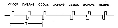 The time "T" is dependent upon whether the computer
is in high speed or low speed. In low speed the time "T" is
2 ms. In high speed this time is 1 ms. This timing results
in a transfer rate of 500 baud and 1000 baud respectively.
The cassette routines are resident in the Level II
ROM's and cassette is accessed as an I/0 port. When a CSAVE
is entered, the address FF is placed on the address bus
along with OUT* (U18-3) going low. The result is that
FFOUT* (U54-11) goes low. When this happens D2 will go high
and will be clocked into U8. This will turn U9 on and
therefore the relay Kl. This shorting of pins 1 and 3 of
the cassette connector through Kl will turn the cassette
motor on. D0 and Dl also get clocked into U8 with timing
that results in the above diagram.
The cassette loading operation is accomplished
through U21 A, B, and C. Refer to the figure below.
CASSETTE WAVEFORMS
The time "T" is dependent upon whether the computer
is in high speed or low speed. In low speed the time "T" is
2 ms. In high speed this time is 1 ms. This timing results
in a transfer rate of 500 baud and 1000 baud respectively.
The cassette routines are resident in the Level II
ROM's and cassette is accessed as an I/0 port. When a CSAVE
is entered, the address FF is placed on the address bus
along with OUT* (U18-3) going low. The result is that
FFOUT* (U54-11) goes low. When this happens D2 will go high
and will be clocked into U8. This will turn U9 on and
therefore the relay Kl. This shorting of pins 1 and 3 of
the cassette connector through Kl will turn the cassette
motor on. D0 and Dl also get clocked into U8 with timing
that results in the above diagram.
The cassette loading operation is accomplished
through U21 A, B, and C. Refer to the figure below.
CASSETTE WAVEFORMS
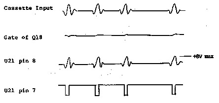 The signal from the cassette is voltage divided by
R24 and R25. U21A is a two pole active high pass filter
which will eliminate noise. U21B along with U18 function as
an automatic gain controlled (AGC) amplifier. The amplitude
at U218 is peak detected by CR2 and C119 to get an average
signal level. The voltage at the gate of Q18 will then be
higher as the signal amplitude goes higher. The higher the
voltage at the gate, the higher the resistance between the
source and drain which will have the effect of lowering the
gain of this stage. The lower the gate voltage, the lower
the drain to
source resistance and the higher the gain. The voltage
level of U21B will be controlled to a maximum of about 8.0
volts. U21C is a comparator who's trip level is dependent
upon the voltage at U2lC pin 5. The output at pin 7 is
normally high which will go low when a data or clock signal
is encountered.
U38 is a flip flop who is set and reset by U21C pin
7 and FFOUT* respectively. The decoded signal FFIN* will
then place the cassette information onto D7.
POWER SUPPLY
The LNW80 power supply section is designed to power
both the LNW80 computer board and the LNW expansion board.
The LNW80 transformer is 9 volts AC rated at 4 amps
and 18 volts AC rated at 2 amps. The unregulated AC voltage
of the transformer is rectified by CR17 and filtered by the
l5,000 ufd capacitor. This capacitor must be located
somewhere off the LNW80 board. Q3, 97, Q8, Q9, and Q10
provide the regulated +5 volt supplies. All +5 volt outputs
are connected through diodes to a summing point at thte
anode of Q12. If any of these voltages exceeds
approximately 6.2V then CR24 will begin to conduct. While
the gate of Q12 remains unchanged, the anode voltage will
begin to rise higher than the gate. This will cause Q12 to
begin conducting which will fire SCR1 causing F1 to open.
This overvoltage protection prevents damaege to components
due to high voltage.
CR15 rectifies the AC signal which is then filtered
by C121. Q4 regulates thte voltage to +12 volts. If the
voltage at JP9 exceeds 13 volts, CR11 will begin to conduct.
While the gate of Q6 remains unchanged, the anode will rise
above the gate voltage. This will cause Q6 to begin
conducting and result in turning SCR2 on and F2 will open.
R138 limits the current, C137 provides DC blocking
and CR19 and CR16 provide a voltage doubler. Q11 will then
provide a -12 volt regulated output which supplies both the
LNW80 computer and expansion board.
The voltage at the negative lead of C131 is
regulated by R133 and CR14 and it is then filtered by C130.
This -5 volts is used both for the LNW80 computer and
expansion board.
TOC | Next Page
The signal from the cassette is voltage divided by
R24 and R25. U21A is a two pole active high pass filter
which will eliminate noise. U21B along with U18 function as
an automatic gain controlled (AGC) amplifier. The amplitude
at U218 is peak detected by CR2 and C119 to get an average
signal level. The voltage at the gate of Q18 will then be
higher as the signal amplitude goes higher. The higher the
voltage at the gate, the higher the resistance between the
source and drain which will have the effect of lowering the
gain of this stage. The lower the gate voltage, the lower
the drain to
source resistance and the higher the gain. The voltage
level of U21B will be controlled to a maximum of about 8.0
volts. U21C is a comparator who's trip level is dependent
upon the voltage at U2lC pin 5. The output at pin 7 is
normally high which will go low when a data or clock signal
is encountered.
U38 is a flip flop who is set and reset by U21C pin
7 and FFOUT* respectively. The decoded signal FFIN* will
then place the cassette information onto D7.
POWER SUPPLY
The LNW80 power supply section is designed to power
both the LNW80 computer board and the LNW expansion board.
The LNW80 transformer is 9 volts AC rated at 4 amps
and 18 volts AC rated at 2 amps. The unregulated AC voltage
of the transformer is rectified by CR17 and filtered by the
l5,000 ufd capacitor. This capacitor must be located
somewhere off the LNW80 board. Q3, 97, Q8, Q9, and Q10
provide the regulated +5 volt supplies. All +5 volt outputs
are connected through diodes to a summing point at thte
anode of Q12. If any of these voltages exceeds
approximately 6.2V then CR24 will begin to conduct. While
the gate of Q12 remains unchanged, the anode voltage will
begin to rise higher than the gate. This will cause Q12 to
begin conducting which will fire SCR1 causing F1 to open.
This overvoltage protection prevents damaege to components
due to high voltage.
CR15 rectifies the AC signal which is then filtered
by C121. Q4 regulates thte voltage to +12 volts. If the
voltage at JP9 exceeds 13 volts, CR11 will begin to conduct.
While the gate of Q6 remains unchanged, the anode will rise
above the gate voltage. This will cause Q6 to begin
conducting and result in turning SCR2 on and F2 will open.
R138 limits the current, C137 provides DC blocking
and CR19 and CR16 provide a voltage doubler. Q11 will then
provide a -12 volt regulated output which supplies both the
LNW80 computer and expansion board.
The voltage at the negative lead of C131 is
regulated by R133 and CR14 and it is then filtered by C130.
This -5 volts is used both for the LNW80 computer and
expansion board.
TOC | Next Page