LNW80 Technical Reference Manual
THEORY OP OPERATIONS
EXPANSION BOARD
The Expansion board is merely an extension of the
main computer board. A number of the functions of the LNW80
Computer are performed on the expansion board. These
functions include additional memory, real time clock, floppy
disk controller, parallel printer, and RS232C serial port.
The expansion bus is a 40 pin connecter that contains all of
the necessary control, data, and address lines necessary for
operation.
LNW80 EXPANSION BUS
The 48 pin bus is equivalent tO the TRS80's 40 pin
expansion bus. The following are the signals and their
descriptions for the expansion bus:
PIN # SIGNAL NAME DESCRIPTION
1 RAS* ROW ADDRESS STROBE
2 SYSRES* SYSTEM RESET
3 CAS* COLUMN ADDRESS STROBE
4 A10 ADDRESS INPUT
5 A12 ADDRESS INPUT
6 A13 ADDRESS INPUT
7 A15 ADDRESS INPUT
8 GND GROUND
9 A11 ADDRESS INPUT
10 A14 ADDRESS INPUT
11 A8 ADDRESS INPUT
12 OUT* I/0 WRITE STROBE
13 WR* WRITE STROBE
14 INTACK* INTERUPT ACKNOWLEDGE
15 RD* READ STROBE
16 MUX ADDRESS MULTIPLEXER
17 A9 ADDRESS INPUT
18 D4 DATA BUS
19 IN* I/0 READ STROBE
20 D7 DATA BUS
21 INT* MASKABLE INTERUPT REQUEST
22 D1 DATA BUS
23 TEST* BUS REQUEST
24 D6 DATA BUS
25 A0 ADDRESS INPUT
26 D3 DATA BUS
27 A1 ADDRESS INPUT
28 D5 DATA BUS
29 GND GROUND
30 D0 DATA BUS
31 A4 ADDRESS INPUT
32 D2 DATA BUS
33 WAIT* Z80A CPU WAIT
34 A3 ADDRESS INPUT
35 A5 ADDRESS INPUT
36 A7 ADDRESS INPUT
37 GND GROUND
38 A6 ADDRESS INPUT
39 GND GROUND
40 A2 ADDRESS INPUT
MEMORY EXPANSION
The Expansion Board contains 16 additional 4116 type
RAM chips at U42-49 and U53-60. U37 and U38 (LS241's) are
used to multiplex the address lines. U34 and U35 are used
to buffer the data lines both input and output.
RAS* is buffered to all of the RAMs while CAS* is
gated by U29 with 48KRAMEN* and 32KRAMEN*. When the CPU
wishes to access the upper memory it places an address from
7FFF to FFFF on the expansion bus. The address is decoded
at U30. When A15 and A14 are high and RAS* is low,
48KRAMEN* (U30-7) will go low enabling CAS* to the upper
bank of memory. When A15 is high and A14 and RAS* are low,
32KRAMEN* (U30-6) will go low enabling CAS* to the lower
bank.
The data bus is buffered by U34 and U35. These buffers
will pass data from the memory onto the data bus when pin 1
of U34 and U35 is low. 32KRAMEN* and 48KRAMEN* are fed into
U11 pins 2 and 1 respectively. When either goes low the
output (U11-3) will go low. This signal is used to gate RD*
through U29 pins 9 and 18 respectively. U29-8 is then fed
into U34 and U35 and is used to enable memory data onto the
data bus. U34 and U35 is tied to gnd thus enabling data
from the data bus to the data input of the memory array at
all times.
For further information on the operation of 4116 type
dynamic rams refer to the section on program memory in the
theory of operations of the LNW80 computer board.
FLOPPY CONTROLLER AND PRINTER DECODING
U19 is used to decode the various signals involved
in the floppy disk and parallel printer circuits. All
addresses memory mapped within the range 37EB to 37EC (HEX)
are decoded through U19.
When the CPU places an address in this range on the
address bus RAS* (U30-1) will go low indicating a valid
address. All of the inputs to U31 will go high resulting in
a logic "0" at U31-8. All, A14, and A15 will be low such
that all of the inputs to U30, pins 1,2,3,13, and 14, will
be low. U30-4 will go low enabling U30-12 which will also go
low. U30-12 is used to enable the outputs of U19 which
effectively produces a "double" 2/4 line decoder.
The outputs of U19 are used as control signals for
both the Floppy Controller and the Parallel Printer
Interfaces. Explanations of these signals and the addresses
that decode them may be found below:
ADDRESS
PIN# FUNCTION DECODE WR* RD*
====================================================
7 INTERUPT RESET 37E0H 1 0
6 N/C 37E4 1 0
5 PRINTER STATUS READ 37E8 1 0
4 FLOPPY READ 37EC 1 0
9 MOTOR ON/DRIVE SELECT 37EH 0 1
10 CASSETTE 37E4 0 1
11 PRINTER WR STROBE 37E8 0 1
12 FLOPPY WRITE 37EC 0 1
PARALLEL LINE PRINTER PORT
The expansion board contains an interface to the
Radio Shack/Centronic Printer. This Printer Interface
consists of an eight bit output port and a four bit input
port.
This I/0 port is accessed by either writing or
reading from address 37E8 Hex. This address is decoded at
U30, U31, and U19.
When reading the memory address 37EB, the printer
status is read through U3. Only the 4 most significant data
bits contain valid information. The meaning of each data
bit is as follows:
Data Bit Printer Status
======== ==============
D7 Printer Busy
D6 Paper Empty
D5 Unit Select
D4 Fault
The Radio Shack's parallel printer has wire ORed
internally, the printer busy status, and the paper empty
signal. When using the Radio Shack/Centronic Printer, only
one of these two bits, D6 or D7, needs to be checked. The
printer busy indication is issued by asserting a logic
When this occurs, the paper empty status will also be a
logic "1". The unit select and fault status bits are not
used by the Radio Shack's printer.
A write to memory location 37EB will load the output
latch U4 and U5 to the line printer's internal data buffer
and also generate a signal through U7 called DATA STROBE
(U7-4). DATA STROBE will be a low-going pulse of
approximately
1.5us.
The Radio Shack's printer is set up to recognize the
following control characters for the line feed and carriage
return:
Character Function
========= ========
0A(Hex) Line Feed
0D Carriage Return
When either of these control characters are received
by the printer, the printer will assert a logic "1" at the
printer busy status.
CLOCK CIRCUIT
The Expansion Board Main Clock is a 4 MHz
oscillator, utilizing Y1 and U18 to form a series resonant
circuit. The 4MHz clock is input to U9-14 and U24-2.
U9 provides a divide by 2 resulting in a 2 MHz clock
at U9-12, which is then input to U22-3 which again divides
by 2 resulting in the 1 MHz clock input to the FLOPPY
CONTROLLER (U14) .
U24 effectively produces a divide by 13 of the 4 MHz
clock resulting in a 307 KHz clock at U24-11. This is used
to clock U25, a 4 bit binary counter. Its output produces 4
of the 8 baud rates used for the SERIAL INTERFACE. The
frequencies of the outputs can be calculated by multiplying
the baud frequency by 16 for the frequency in Hz.
U17 is clocked by U25-12 (30.4KHz) and provides a
divide by 11 resulting in a 3.49KHz clock at U17-11. This
is input to U10-14, which does a divide by two such that
U10-12 is a 1.75KHz clock.
The 2nd half of U10 is clocked by U25-11 (19.2KHz)
and does a divide by 8. The outputs of U10 provide the
other 4 baud rate clock signals. Baud rate clocks will be
discussed in the section entitled "SERIAL INTERFACE".
U10-11 (2.4KHz) is clocked into U9-1 which set for a
divide by 6 resulting in an output of 400Hz. This is then
input to U12 which is set for a divide by ten resulting in
the 40Hz clock signal used to provide the REAL TIME CLOCK.
FLOPPY DISK INTERFACE
The function of interfacing to a floppy disk drive
is performed primarily by the Western Digital's FD1771B-01
Floppy Disk Formatter/Controller chip. Note that when using
double density adapters, the "doubler" performs the duties
of the controller chip. The LNDOUBLER 5/8 will be explained
in a further section.
The FD1771, a MOS/LSI device which performs much of
the housekeeping involved in reading and writing data to and
from the disk has the following internal features:
1. Cyclic redundancy check and generation for error
checking.
2. Internally seperates disk head outpput into data.
3. Checks for desired section, check ID field and
locate it's data address mark.
4. Accounts for track number of the current
read/write head position
The interface to the processor is accomplished
through the eight Data Access Line (DAL) and the associated
control signals.
When reading from the DAL, the address decoder U19-4
(37EC READ*) will be low enabling U8 and U15 to buffer data
from U14 to the data bus. U8 and U15 are LS240's, OCTAL
BUFFERS/LINE DRIVERS/LINE RECEIVERS with inverted 3-state
outputs.
When writing from the data bus to the DAL, the
address decoder U19-12 (37EC WRITE*) will be low enabling U8
and U15 to buffer data from the data bus to the floppy
controller.
The least two significant addresses, A0 and A1, are
decoded by the floppy controller to interpret the selected
registers of the read and write operations. These registers
are decoded as follows:
A1-A0 READ WRITE
===== ========== ===========
0 0 STATUS REG. COMMAND REG.
0 1 TRACK REG. TRACK REG.
1 0 SECTOR REG. SECTOR REG.
1 1 DATA REG. DATA REG.
The interrupt request (INTRQ) of the FDC (U14-39)
indicates the completion or termination of any operation.
INTRQ presets U22A presenting a high to Ul pins 4 and 5,
which is reset by reading the FDC Status Register. Reading
from 37E0H will reset the interrupt signal (Ul-6) by clocking
a low at the output of U22A.
The FDC requires a 1 MHz clock input to U14-24 which
is generated from the 4 MHz main clack circuit and is
explained in the clock discription of the expansion board.
Drive Selection through Data Lines DH-D3 is clocked
into U13 by 37E8 WRITE* (U19-9). This also triggers the
one-shot, U7A, generating the motor on signal. The drive
selection is only activated when the motor on signal (U7-5)
is high.
When U7-5 is low, clearing U13, a high is generated
at U11-8. This signal is then inverted at U20-10 providing
a low command and indicating that the floppy status is
ready.
U14-19 is the MASTER RESET, and is driven by SYSRES*
from the main computer board. When WR* goes low, the FDC is
reset and HEX 03 is loaded into the command register and the
system will proceed to reboot. For further details of the
internal operations and the programing of the FDC refer to
the data sheets.
SERIAL INTERFACE
The Block Diagram (figure 8) outlines the major
sections of the Serial Interface. For the following circuit
description, use the schmatics along with the Block Diagram
to aid in visualizing the circuit theory.
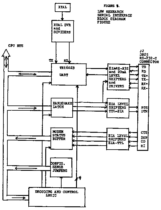 BAUD RATE GENERATION
In order to provide the receive and transmit baud
clocks for the UART, the 4 MHz clock is divided down.
Details of the clock divider circuitry is given in the
section entitled CLOCK CIRCUIT.
The Baud Rate is programmed by jumpering
A,B,C,D,E,F,G, or H to the RX and TX line. (Note that on
the pre-assembled LNW80 Systems, these have been jumpered
using two 8-pin dip switches.) These RX and TX lines are
used by the UART far the RECEIVE and TRANSMIT BAUD CLOCKS.
TR1602B UART
The TR1602B Universal Asynchronoous
Receiver/Transmitter (UART) is the heart of the serial
interface. It takes parallel data from the CPU BUS and
converts it to serial data and at the same time can receive
serial data and convert it to parallel. It has two
registers which can be read--one for the status and the
other with received data. It has two registers which can be
loaded--one with transmit data and the other with control
information (word length,parity,stop bits). Refer to the
Data Sheet of the Western Digital TR1602B for further
details of operation.
EIA RS232C and 20mA LEVEL SHIFTERS AND DRIVERS
The serial output of U40 is pin25 (TRQ). It drives
U18 for buffering to EIA Driver U61-9 and the 20mA driver
U50-6. Serial data can be output by U26-10 which drives
both U50-7 and U61-10. U50, R23, and R24 provide the 20mA
interface. When U50 conducts it allows about 20mA of
current to flow (20mA=mark,0mA=space). Received serial data
is brought in to U51-4. U51 is an EIA to TTL receiver. The
20mA serial input is accomplished by the current to voltage
conversion of R25 and R26. The TTL received data is fed to
the Receive Data (RI,U40-20) of the UART and is fed to
U33-12 to, be read as part of the Modem Status Buffer.
HANDSHAKE LATCH
U26 is the handshake latch. D0-D2 inputs to U26
pins 4, 5, and 12 respectively. The latch is loaded when
OUT EAH (U16-5) goes low which is input to U26-9. The
outputs of U26 are fed to U61-12,13 and U61-4,5 for level
conversion to EIA standards.
MODEM STATUS BUFFER
U33 is the modem status buffer. U52, an EIA
receiver, converts EIA levels to TTL. This is input to U33
and enabled to the data bus when IN E8H (U16-7) goes low.
In addition, the Serial Input (TTL) is fed to U33-12 to
allow the CPU to directly input the serial data.
CONFIGURATION SENSE JUMPERS
Jumper wires from K,N,P,M, and J connected to E5 or
E6 select whether the associated data bit is a "1" or a "0"
when U28 is enabled onto the data bus. It is enabled by IN
E9H (U16-6) and is used by serial driver programs so that
stop bits, parity, and word length can be selected by
hardware configuration.
DECODING AND CONTROL LOGIC
The port address decoding (IN,OUT-E8,E9,EA,EB) is
accomplished by U4l and U16. U41 decades the upper 6 bits
(E8) and outputs to the strobe inputs of U16. The lower two
address bits (A1,A0) feed to the A and B inputs of U16. U16
is a 2/4 line decoder and its outputs. (active low) select
which part is addressed and whether it is an IN or OUT
instruction. U23 pins 1 and 2 are driven by INEAH and INEBH
such that whenever the Receive Register and the Status
Regiser of the UART are read, U39 drives the data onto the
data bus. Below is a summary of the address decoding:
IN E8H - Modum Status Register
IN E9H - Configuration Jumpers
IN EAH - UART Status Register
IN EBH - UART Receive Register, Data Received Reset
OUT E8H - Master Reset
OUT E9H - Not Used
OUT EAH - Control Register Load, Handshake Latch Load
OUT EBH - Transmit Holding Register Load
SERIAL INTERFACE PORT ADDRESSING
BAUD RATE GENERATION
In order to provide the receive and transmit baud
clocks for the UART, the 4 MHz clock is divided down.
Details of the clock divider circuitry is given in the
section entitled CLOCK CIRCUIT.
The Baud Rate is programmed by jumpering
A,B,C,D,E,F,G, or H to the RX and TX line. (Note that on
the pre-assembled LNW80 Systems, these have been jumpered
using two 8-pin dip switches.) These RX and TX lines are
used by the UART far the RECEIVE and TRANSMIT BAUD CLOCKS.
TR1602B UART
The TR1602B Universal Asynchronoous
Receiver/Transmitter (UART) is the heart of the serial
interface. It takes parallel data from the CPU BUS and
converts it to serial data and at the same time can receive
serial data and convert it to parallel. It has two
registers which can be read--one for the status and the
other with received data. It has two registers which can be
loaded--one with transmit data and the other with control
information (word length,parity,stop bits). Refer to the
Data Sheet of the Western Digital TR1602B for further
details of operation.
EIA RS232C and 20mA LEVEL SHIFTERS AND DRIVERS
The serial output of U40 is pin25 (TRQ). It drives
U18 for buffering to EIA Driver U61-9 and the 20mA driver
U50-6. Serial data can be output by U26-10 which drives
both U50-7 and U61-10. U50, R23, and R24 provide the 20mA
interface. When U50 conducts it allows about 20mA of
current to flow (20mA=mark,0mA=space). Received serial data
is brought in to U51-4. U51 is an EIA to TTL receiver. The
20mA serial input is accomplished by the current to voltage
conversion of R25 and R26. The TTL received data is fed to
the Receive Data (RI,U40-20) of the UART and is fed to
U33-12 to, be read as part of the Modem Status Buffer.
HANDSHAKE LATCH
U26 is the handshake latch. D0-D2 inputs to U26
pins 4, 5, and 12 respectively. The latch is loaded when
OUT EAH (U16-5) goes low which is input to U26-9. The
outputs of U26 are fed to U61-12,13 and U61-4,5 for level
conversion to EIA standards.
MODEM STATUS BUFFER
U33 is the modem status buffer. U52, an EIA
receiver, converts EIA levels to TTL. This is input to U33
and enabled to the data bus when IN E8H (U16-7) goes low.
In addition, the Serial Input (TTL) is fed to U33-12 to
allow the CPU to directly input the serial data.
CONFIGURATION SENSE JUMPERS
Jumper wires from K,N,P,M, and J connected to E5 or
E6 select whether the associated data bit is a "1" or a "0"
when U28 is enabled onto the data bus. It is enabled by IN
E9H (U16-6) and is used by serial driver programs so that
stop bits, parity, and word length can be selected by
hardware configuration.
DECODING AND CONTROL LOGIC
The port address decoding (IN,OUT-E8,E9,EA,EB) is
accomplished by U4l and U16. U41 decades the upper 6 bits
(E8) and outputs to the strobe inputs of U16. The lower two
address bits (A1,A0) feed to the A and B inputs of U16. U16
is a 2/4 line decoder and its outputs. (active low) select
which part is addressed and whether it is an IN or OUT
instruction. U23 pins 1 and 2 are driven by INEAH and INEBH
such that whenever the Receive Register and the Status
Regiser of the UART are read, U39 drives the data onto the
data bus. Below is a summary of the address decoding:
IN E8H - Modum Status Register
IN E9H - Configuration Jumpers
IN EAH - UART Status Register
IN EBH - UART Receive Register, Data Received Reset
OUT E8H - Master Reset
OUT E9H - Not Used
OUT EAH - Control Register Load, Handshake Latch Load
OUT EBH - Transmit Holding Register Load
SERIAL INTERFACE PORT ADDRESSING
Data
Bit | Jumper
Letter | Configuration
Jumpers | UART Control
Register
Handshake Latch | UART Status
Register | Modem Status
Register |
| D7 | j | Even/0dd Parity
1=Even 0=Odd | Even/Odd Parity | Data Receive
1=True | Clear to send
Pin 5 DB-25 |
| D6 | m | Word Length 1 | Word Length 1 | THRE 1=True | DSR
Pin 6 DB-25 |
| D5 | p | Word Length 2 | Word Length 2 | OverrunError
1=True | CD
Pin 8 DB-25 |
D4nStop Bit Slct.
1=2bits,O=lbitStop Bit Slct.
1=2bits,O=1bitFraming Err.
1=True | Ring Indctor.
Pin 22 DB-25 | |
| | | |
| D3 | k | Parity Inhibit
1 disabled par. | Parity Inhibit
1 disabled par. | Parity Error
1=True |
| D2 | | | Break, 0 Disable
Transmit Data |
| D1 | | | Request to Send
Pin 4 DB-25 | | Receiver In.
UART Pin 20 |
| D0 | | | Data Terminal
Ready
Pin 20 DB-25 |
| | IN 0E9H | OUT 0EAH | IN 0EAH | IN 0E8H |
REAL TIME CLOCK

        The 40 Hz Real Time Clock is output from U12-11 and
used to clock U21B.  This clocks a logic "0" to U21-9 which
presets U21A.  This places a logic "1" at U21-5 which is
input t0 U29-4.  If U29-4 goes high then its output U29-6
will go high.  U29-6 is inverted through U20 and thus
presets U22B.  U22-9 goes high and is inverted through U1


which sends a maskable interupt request to the CPU.  The CPU
responds by decoding 37E0RD* at U19-7.  37E0RD* presents
U21B, clocks a logic "0" into U21A, and enables the output
of U38.  If bit D7 is a logic "1", then the RTC generated
the interupt request.

        The programming of the Real Time Clock can be by DOS
or in a User's Machine Program.  Note the DOS Manual for
commands.


                      TOC | Next Page