LNW80 Technical Reference Manual
LNW8O MICRO COMPUTER
TECHNICAL REFERENCE MANUAL
BY
DAVID L. KELLY
FIRST EDITION - 1982
All rights reserved. Reproduction or
use, without express permission is
prohibited. While every effort was taken
in the preparation of this book, the
publisher assumes no liability for
errors or omissions. Neither is any
liability assumed far damages resulting
from the use of the information
contained herein.
Copyright(C)1982, LNW RESEARCH CORP.
CONTENTS
PAGE
I. SYSTEM OVERVIEW.......................................1
CENTRAL PROCESSING UNIT...............................1
READ ONLY MEMORY......................................1
RANDOM ACCESS MEMORY..................................2
KEYBOARD..............................................2
VIDEO & VIDEO PROCESSING..............................2
TAPE INTERFACE........................................3
SERIAL INTERFACE......................................3
FLOPPY DISK CONTROLLER................................3
II. THEORY OF OPERATIONS LNW80 BOARD......................4
SYSTEM CLOCK..........................................4
CPU ADDRESS LINES.....................................4
CPU DATA BUS..........................................5
WAIT*, INT*, & TEST*..................................5
CPU CONTROL SIGNALS...................................6
ADDRESS DECODING CIRCUIT..............................6
LNW80 MEMORY MAP......................................7
READ ONLY MEMORY......................................7
PROGRAM RAM...........................................8
KEYBOARD..............................................9
VIDEO DIVIDER CHAIN..................................10
VIDEO RAM ADDRESSING.................................14
LOW RESOLUTION VIDEO RAM.............................15
HI RESOLUTION GRAPHICS RAM...........................17
VIDEO DATA LATCH.....................................18
CHARACTER GENERATOR..................................19
GRAPHICS GENERATOR...................................19
ALPHA NUMERIC/GRAPHIC SHIFT REGISTERS................20
INVERSE VIDEO........................................21
HORIZONTAL & VERTICAL SYNC TIMING....................21
COMPOSITE VIDEO MIXING CIRCUITS......................22
NTSC COLOR VIDEO.....................................23
COLOR BURST ONE-SHOT.................................26
U146 - MC1372 COLOR ENCODER..........................26
HI RESOLUTION COLOR..................................27
BLACK & WHITE THRU NTSC CHANNEL......................27
CASSETTE.............................................27
POWER................................................29
III. THEORY OPERATIONS EXPANSION BOARD....................30
EXPANSION BUS........................................31
MEMORY EXPANSION.....................................32
FLOPPY CONTROLLER & PRINTER DECODING.................32
PARALLEL LINE PRINTER PORT...........................33
CLOCK CIRCUIT........................................34
FLOPPY DISK INTERFACE................................35
SERIAL INTERFACE.....................................36
BAUD RATE GENERATION.................................38
TR1602B UART.........................................38
E1A RS232C & 20 mA LEVEL SHIFTS & RECEIVERS..........38
HANDSHAKE LATCH......................................38
MODEM STATUS BUFFER..................................39
CONFIGURATION SENSE JUMPERS..........................39
DECODING 4 LOGIC CONTROL.............................39
SERIAL INTERFACE PORT ADDRESSING.....................40
REAL TIME CLOCK......................................40
IV. THEORY OPERATIONS 5/8 DOUBLER........................42
SINGLE/DOUBLE DENSITY OPERATION......................42
CLOCK CIRCUIT.......................................
5.25" & 8" SELECTION/OPERATION.......................43
ANALOG PHASE LOCK LOOP DATA SEPERATION...............44
PRECISION WRITE PRECOMPENSATION......................44
WAIT LOGIC...........................................44
V. TROUBLESHOOTING......................................46
POWER SUPPLY.........................................46
VIDEO OUTPUT/ADJUSTMENTS.............................46
SYSTEM CLOCK.........................................46
CPU/CPU TEST.........................................47
CPU/CPU TEST PROGRAM.................................48
SCOTCH TAPE TRICK....................................50
HI RESOLUTION GRAPHICS...............................50
HI RESOLUTION GRAPHICS TEST..........................51
COLOR GRAPHICS TEST & ADJUSTMENT.....................52
VI. TROUBLESHOOTING THE EXPANSION INTERFACE..............53
POWER SUPPLY.........................................53
32K MEMORY EXPANSION.................................53
FLOPPY DISK CONTROLLER...............................54
RS232 SERIAL PORT....................................54
SERIAL CIRCUIT TERMINAL PROGRAM......................55
SERIAL PRINTER DRIVER PROGRAM........................55
VII. 5/8 DOUBLER ALIGNMENT................................57
VIII. DISASSEMBLY/ASSEMBLY.................................58
REMOVING THE LID.....................................58
REMOVING THE KEYBOARD................................58
REMOVING THE EXPANSION INTERFACE.....................58
REMOVING THE LNDOUBLER 5/8...........................59
REMOVING THE LNW80 COMPUTER BOARD....................59
REASSEMBLING THE COMPUTER............................59
IX. ENGINEERING CHANGE NOTICES...........................60
X. RGB OPTION...........................................65
RGB CIRCUIT DIAGRAM..................................66
XI. PARTS LIST LNW80 COMPUTER BOARD......................67
XII. PARTS LIST EXPANSION INTERFACE.......................78
XIII. PARTS LIST 5/8 DOUBLER...............................83
XIV. PARTS LIST CASE ASSEMBLY.............................85
XV. APPENDIX 1 - DATA SHEETS.............................86
XVI. APPENDIX 2 - ENGINEERING DRAWINGS...................184
INTRODUCTION
This book was written for those people who
have the technical knowledge to understand how a
computer operates. This requires that the reader
has a through understanding of digital logic.
Armed with a TTL DATA BOOK and this manual such a
person can understand the complex internal
operation of the LNW80 COMPUTER.
Remember that any work you do to your LNW8O
voids all warranties, implied or expressed. Also
we will not repair or correct owner modifications.
We cannot possibly support owner hardware/circuit
ideas on how to customize the LNW80.
In the following sections refer closely to
the schematics and the system block diagram which
can be found at the end of the manual. Good luck
and have fun.
SYSTEM OVERVIEW
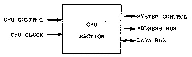
CENTRAL PROCESSING UNIT (CPU)
The heart of the LNW80 is the Z80A CPU. The Z80A
has 16 address lines and therefore 65536 addressable memory
locations. The Z80A receives instructions from the ROM or
RAM and proceeds to execute them. Only the CPU interacts
with all other sections within the computer. The CPU
section includes not only the Z80A but also the data and
address buffers, wait logic, and system control logic.
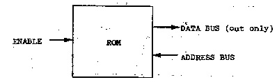
 READ ONLY MEMORY (ROM)
The ROM contains non-erasable data that is used to
provide the CPU with instructions necessary for the system's
operation. Upon power up the CPU outputs to the ROM for its
first instruction after which the ROM takes over and
instructs the CPU exactly how to perform the necessary
funtions to get the system operating.
READ ONLY MEMORY (ROM)
The ROM contains non-erasable data that is used to
provide the CPU with instructions necessary for the system's
operation. Upon power up the CPU outputs to the ROM for its
first instruction after which the ROM takes over and
instructs the CPU exactly how to perform the necessary
funtions to get the system operating.
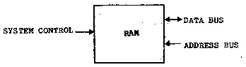
 RANDOM ACCESS MEMORY (RAM)
The RAM is where the CPU stores data. This data may
consist of program information. The RAM differs from the
ROM in that data may be written to as well as read from the
RAM by the CPU.
RANDOM ACCESS MEMORY (RAM)
The RAM is where the CPU stores data. This data may
consist of program information. The RAM differs from the
ROM in that data may be written to as well as read from the
RAM by the CPU.
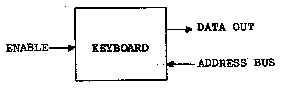
 KEYBOARD
The keyboard is used to input instructions from the
user to the CPU.
KEYBOARD
The keyboard is used to input instructions from the
user to the CPU.
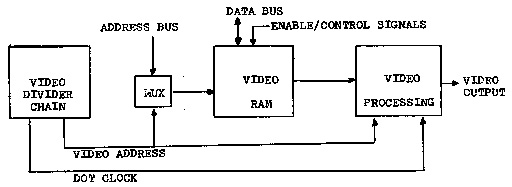
 VIDEO RAM AND PROCESSING
The video is used to inform the user what the system
is doing. All data that is stored in the video ram is
automatically displayed on the CRT by the video processing
unit. The data within the video ram is stored in ASCII.
utilizing the Character Generator the ASCII is translated
into a dot pattern that represents the desired character.
VIDEO RAM AND PROCESSING
The video is used to inform the user what the system
is doing. All data that is stored in the video ram is
automatically displayed on the CRT by the video processing
unit. The data within the video ram is stored in ASCII.
utilizing the Character Generator the ASCII is translated
into a dot pattern that represents the desired character.
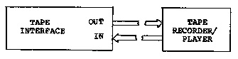
 TAPE INTERFACE
The tape interface stores data on tape so that it
can be recovered at a later date.
TAPE INTERFACE
The tape interface stores data on tape so that it
can be recovered at a later date.
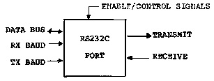
 SERIAL INTERFACE
The RS232C serial interface sends and receives data
in serial fashion and converts that data to parallel form to
be received by the CPU. This section is used to connect to
such devices as modems and serial printers.
SERIAL INTERFACE
The RS232C serial interface sends and receives data
in serial fashion and converts that data to parallel form to
be received by the CPU. This section is used to connect to
such devices as modems and serial printers.
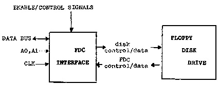
 FLOPPY DISK CONTROLLER (FDC)
The FDC stores large amounts of data and thus
increases the storage capacity of the system.
FLOPPY DISK CONTROLLER (FDC)
The FDC stores large amounts of data and thus
increases the storage capacity of the system.
 TOC | Next Page