The following information is from the
Intel 1981 Component Data Catalog page 3-6 and 3-7.
Note that this is "Preliminary" info :-).
I skipped the BLOCK DIAGRAM, PIN CONFIGURATION, PACKAGE OUTLINE, SOCKET OUTLINE, PIN DESCRIPTION and the boring ABSOLUTE MAXIMUM RATINGS, D.C. AND OPERATING CHARACTERISTICS, DRIVE REQUIREMENTS and CONTROL PULSE REQUIREMENTS
|
|
The Intel Magnetics 7110 is a very high density 1 megabit non-volatile, solid-state memory utilizing the magnetic bubble technology. The usable data storage capacity is 1,048,576 bits. The defect tolerant design incorporates redundant storage loops. The gross capacity of Intel Magnetics bubble memory is 1,310,720 bits.
The 7110 has a true binary organization to simplify system design, interfacing, and system software. The device is organized as 256 data storage loops each having 4096 storage bits. When used with Intel Magnetics complete family of support electronics the resultant minimum system is configured as 128K bytes of usable data storage. The support circuits also provide automatic error correction and transparent handling of redundant loops.
The 7110 has a major track-minor loop architecture; It has separate read and write tracks. Logically, the data is organized as a 512 bit page with a total of 2048 pages. The redundant loop information is stored on-chip in the bootstrap loop along with an index address code. When power is disconnected, the 7110 retains the data stored and the bubble memory system is restarted when power is restored via the support electronics under software control.
The 7110 is packaged in a dual in-line leadless package complete with permanent magnets and coils for the in-plane rotating field. In addition, the 7110 has a magnetic shield surrounding the bubble memory chip to protect the data from externally induced magnetic fields. The 7110 operating data rate is 100 Kbit/sec. The 7110 can be operated asynchronously and has start/stop capability.
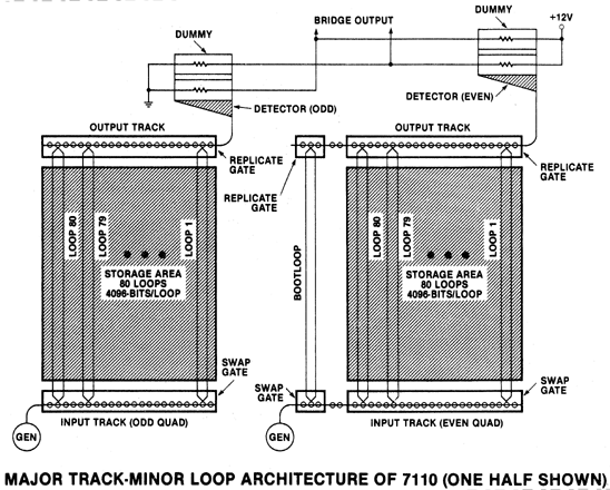
The Intel Magnetics 7110 is a 1 megabit bubble memory module organized as two identical 512K binary half sections. See Major Track-Minor Loop architecture diagram. Each half section is in turn organized as two 256K subsections referred to as quads.
The module consists of a bubble die mounted in a substrate that accommodates two orthogonal drive coils that surround the die. The drive coils produce a rotating magnetic field in the plane of the die when they are excited by 90ş phase shifted triangular current waveforms. The rotating in-plane field is responsible for bubble propagation. One drive field rotation propagates all bubbles in the device one storage location (or cycle). The die-substrate-coil sub-assembly is enclosed in a package consisting of permanent magnets and a shield. The shield serves as a flux return path for the permanent magnets in addition to isolating the device from stray magnetic fields. The permanent magnets produce a bias field that is nearly perpendicular to the plane of the die. This field supports the existence of the bubble domains.
The package is constructed to maintain a 2.5 degree tilt between the plane of the bias magnet faces and the plane of the die. This serves to introduce a small component of the bias field into the plane of the die. During operation when the drive coils are energized this small in-plane component is negligible. During standby or when power is removed the small inplane field ensures that the bubbles will be confined to their appropriate storage locations. The direction of the in-plane field introduced by the package tilt (holding field) is coincident with the 0o phase direction of the drive field.
A 7110 quad sub-section is composed of the following elements shown on the architecture diagram.
The boot loop is read from and written into via the same input and output tracks as the main storage loops. However, it has independently accessed swap and replicate gates. The boot swap, under normal circumstances, is intended only to be used during basic initialization at the factory at which time loop mask and synchronization codes are written. The boot replicate is intended to be accessed every time power is applied to the bubble module and its peripheral control electronics. At such a time, the control electronics would read and store the mask information, plus utilize the synchronization information to establish the location of the data circulating within the loops.
Generic links: