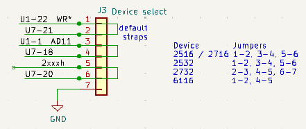
The U7 socket has two intended usages:
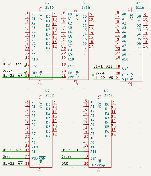
The schematic (Appendix B, User Manual) is very confusing. The default board traces are for 2kByte RAM or 2516/2532 EPROMs. Other settings require cutting traces and setting jumpers.
Jumper J1 allows configuring the socket for three options; RAM and two types of EPROM. Three pins are different:
The J1 connections per usage:
RAM chips of 4 kByte are very uncommon, but a board with two 2 kByte RAM chips exists, adding a battery backup and a write protect. For this situation, configure the socket as for a 2732 and connect J1-1 to the write enable of the board.
The standard MPF-I uses one I/O-device, the 8255 PPI. There are sockets for the Z80 PIO and Z80 CTC. These three devices use threee-quarters of the I/O-space, due to incomplete decoding on the board. This means only 64 ports are available for the extra boards and the BREAD BOARD / USER AREA. This minor modification frees up lots of I/O-space and uses only one additional TTL IC. The I/O-devices remain available on the documented ports, so all software that only uses those ports will be working. The monitor ROM only addresses the 8255 PPI.
This modification also makes the MPF-I(B) somewhat more compatible with the MPF-IP and its extension boards, as the IOM-MPF-P uses the 6xh range for UART and CTC2.
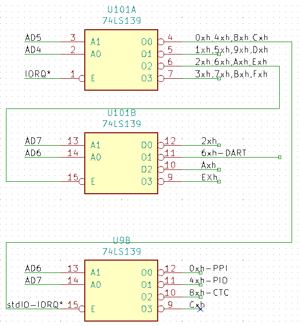
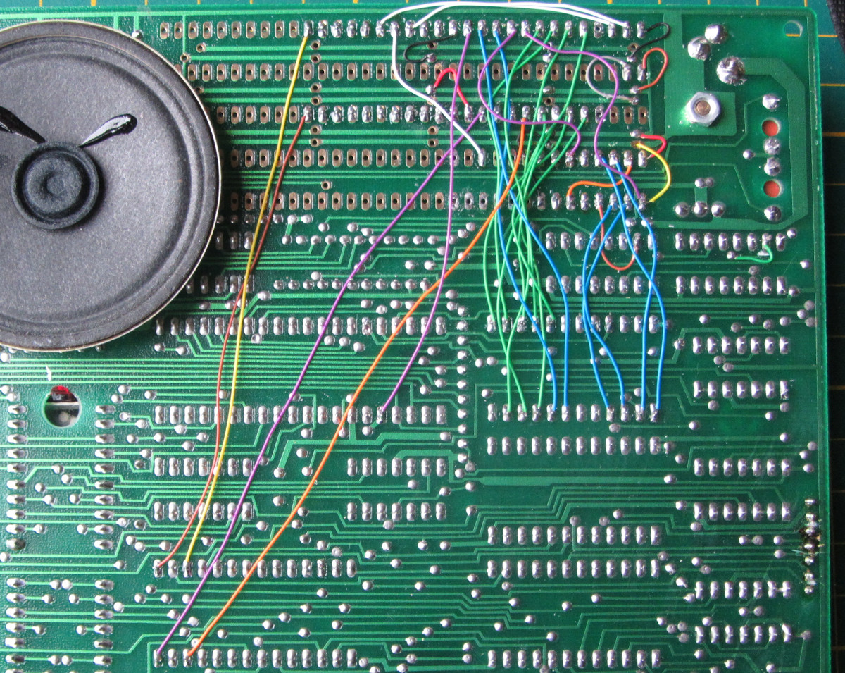
One trace on the MPF-PCB must be cut to add the extra selection. It is the trace between U8 and U9, leading between pins U9-2 and U9-3 to U9-15 (see red arrow on image below). This is the IORQ* signal from the processor to the I/O-port selector. By inserting another selector with address lines AD4 and AD5, the address space of all I/O-devices is reduced from 64 ports to 16. PPI will be 0xh, PIO will be 4xh, CTC will be 8xh. This frees up I/O ranges 10h-3Fh, 50h-7Fh and 90h-BFh for other devices. Each device still uses 16 ports, while 4 would be sufficient, but fixing this would lead to a more complex circuit and be overkill for most usages.
The middle part of the diagram with U101B , AD7 and AD6 is optional and not implemented yet.
![]()
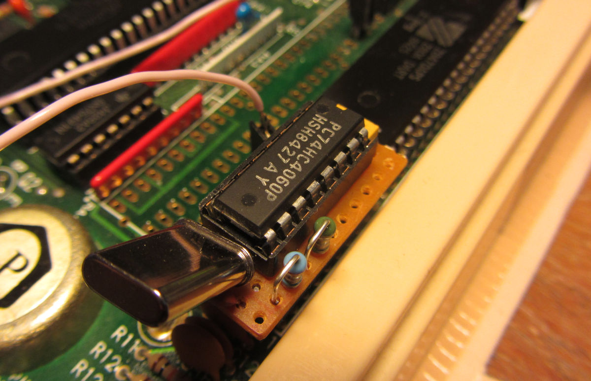
The trace to cut is between the U8 RAM and the U9 74LS139. A wire (yellow) is soldered on the trace-part coming from the processor. A via-pad on the BB-user area is the simplest way to get it to the solder side.
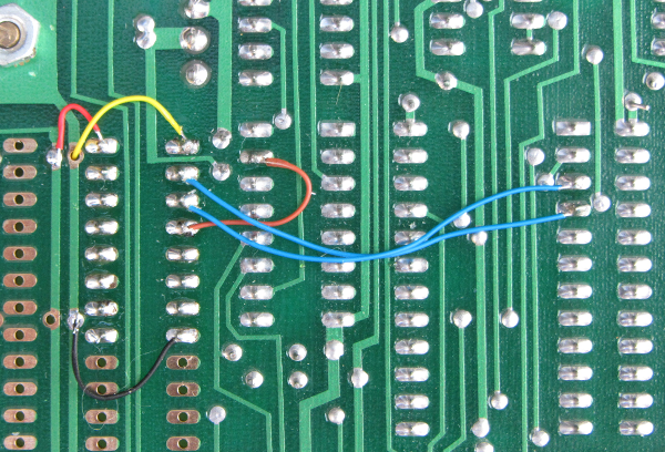
The yellow wire is soldered to pin 1 of the new 74LS139. The lines 2 and 3 are soldered to A4 and A5 of the U8 RAM (pin 4 resp. pin 3). The brown wire complets the connection to pin 15 of the U9 74LS139. Red and black add +5V and ground to the new 74LS139.
The other half of the new 74LS139 can be used for I/O ports on the BB-User space, as shown on the diagram above. The 74LS139 can be replaced with a more modern 74HCT139.
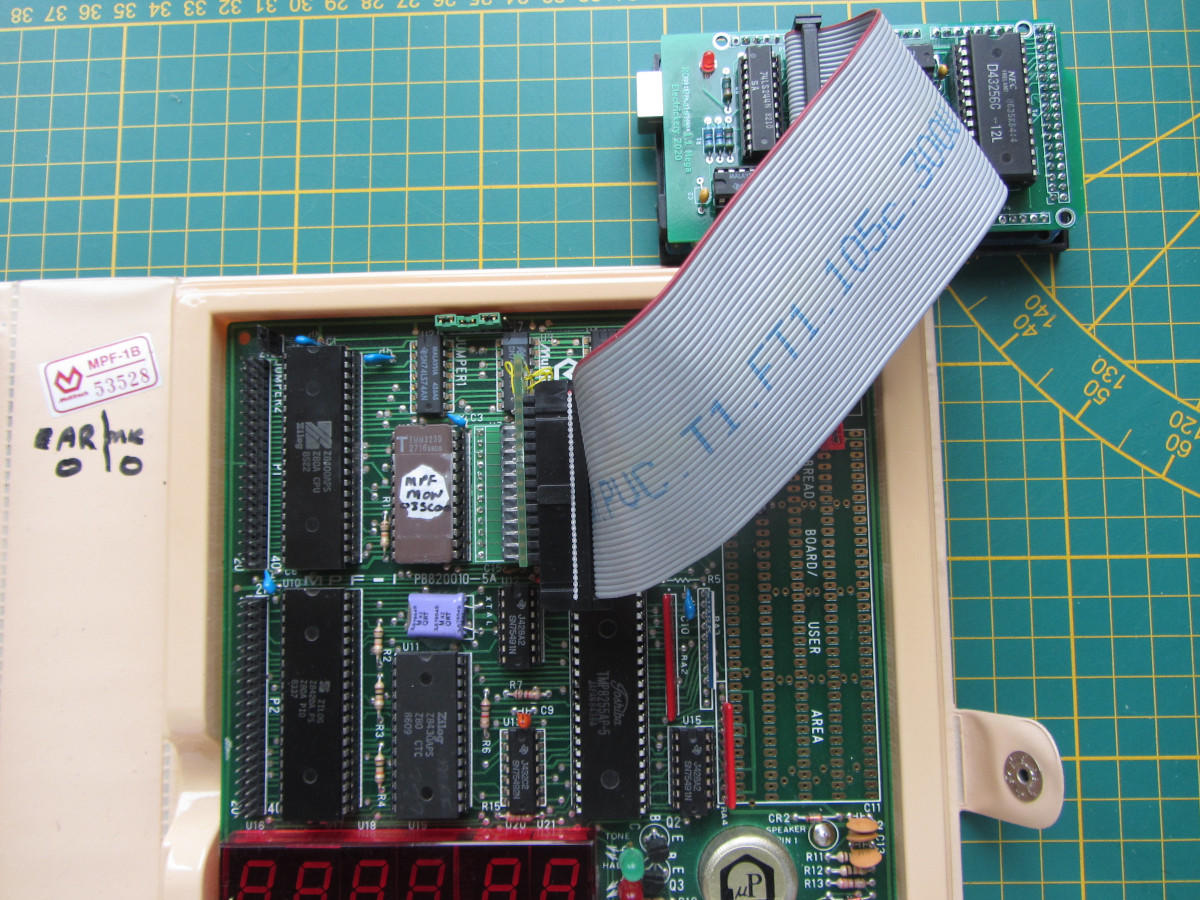
With typical MPF-1 usage in mind, I made an Arduino Mega 2560 based ROM/RAM-emulator. This allows to write data (manual or Intel-Hex formatted) to a RAM in the MPF memory space. In this case the socket U7 which is located at 2000h-2FFFh. With the proper hardware configuration it is a RAM for the MPF.
More info on the ROM/RAM emulator at:
Local
Hackaday
An even more convenient way to transfer code to the MPF-1 is data-transfer under control of the processor. A serial interface and support for Intel HEX allows you to transfer data in the whole Z80 address range. In step is adding a serial chip. The TTL-level signals from this chip can be fed directly into a USB-serial converter, skipping the old-style RS-232C voltage levels. The design is here. The Rx/Tx/GND pins are at the top left, next to the fan-connector.
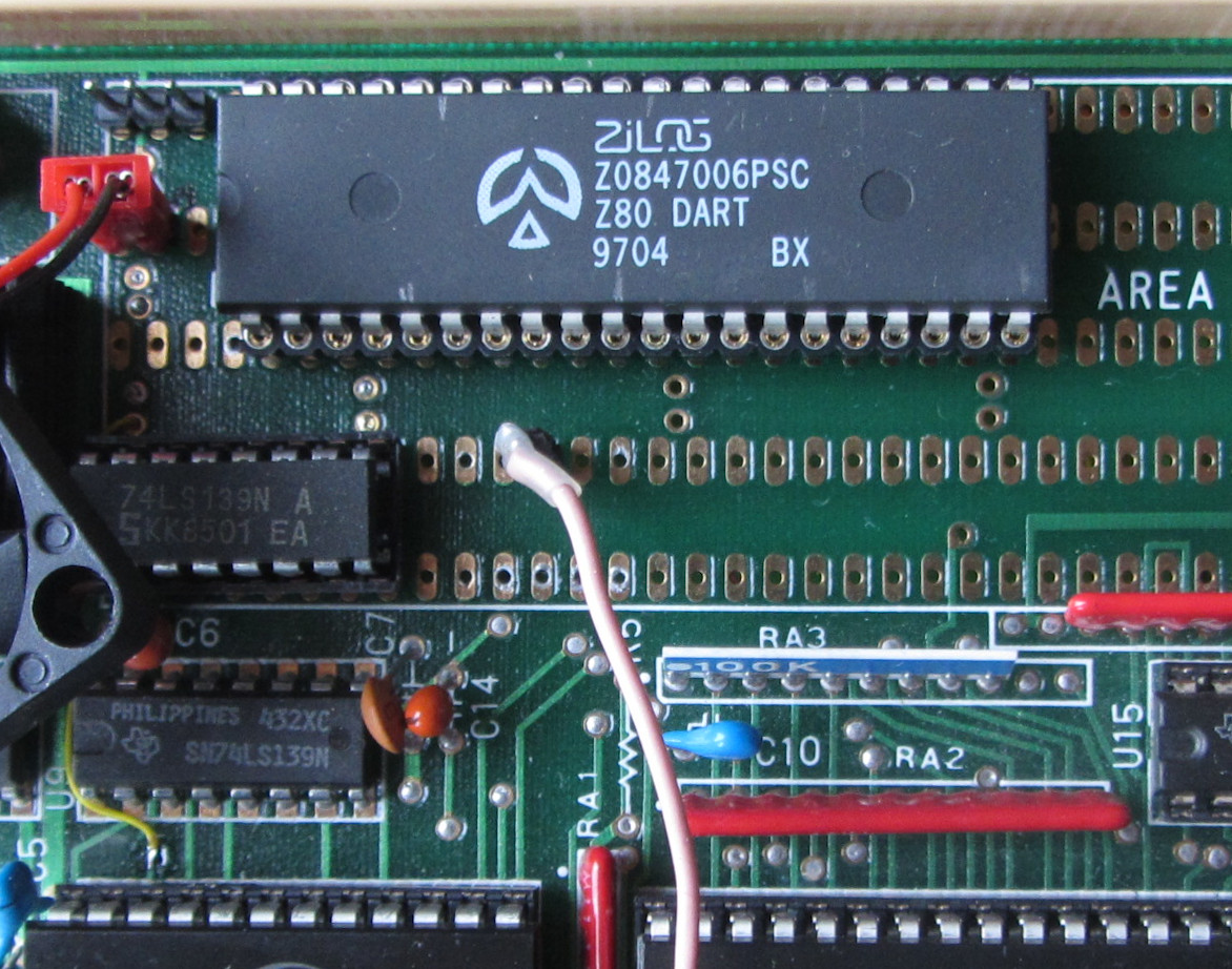
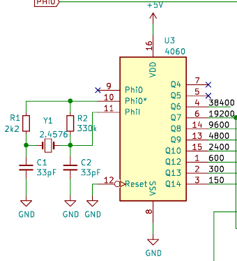
Currently a CTC channel is used to generate the Baud rate (pink wire), but I will probably add a dedicated chip for this. The DART is tested with a very simple program. Next step is porting a simple serial monitor program and start debugging.
A baudrate generator for 9600 Baud was added to complete the onboard serial port. The monitor software is still in ROMEmulator memory.
Last update: 2024-10-12