7.
MICROCOMPUTER
Introduction
The DAI Personal Computer's processor section is designed around the 8080A Microprocessor. The design is based upon the popular and economical high performance DCE microcomputer architecture. The microcomputer section consists of the microprocessor and timing circuitry; the ROM and Static RAM memory; Interrupt Control and Interval Timer logic; and the Master RAM memory. The Master Ram memory consists of a dynamic memory that is configurable from SK bytes up to 48K bytes.
Memory Usage
The DAI Personal Computer's memory space is organised on the basis of memory mapped input-output which allocates normal memory addresses to all I/0 operations alongside the RAM and ROM memory addresses that are required for normal system operation. In the following descriptions the address space is described in terms of hexadecimal numbers where the available range of 64 kilobytes is represented by the address range 0000 to FFFF. Switched banks represent a duplication of addresses.
| 0000 - 003F | INTERRUPT VECTOR | |
| 0040 | CONTROL OUTPUT IMAGE | |
| 0041 - 0061 | UTILITY WORK AREA | |
| 0062 - 0071 | UTILITY INTERRUPT VECTOR. | |
| 0077 - 00CF | SCREEN VARIABLES | |
| 00D0 - 00FF | MATH WORK AREA |
8.
| 0100 - O2EB | BASIC VARIABLES | |
| 02EC | ||
| TO | HEAP(STRINGS + ARRAYS) | |
| TOP OF RAM | ||
| (VARIABLE BOUNDARIES) | PROGRAM (COMPILED BASIC) | |
| SYMBOL TABLE | ||
| NOT USED RAM | ||
| SCREEN DISPLAY | ||
| F800 - F8FF | µC STACK |
The following two byte variables are maintained by the system, Addresses are stored on low order byte, high order byte (8080A)
| Address (Hex) | Variable | |
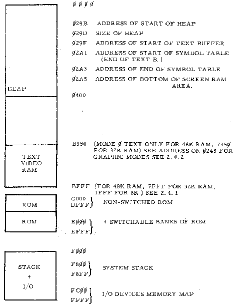
| 029B | START OF HEAP | |
| 029D | SIZE OF HEAP | |
| 029F | START OF PROGRAM BUFFER | |
| 02A1 | END PROGRAM BUFFER AND START-SYMBOL TABLE | |
| 02A3 | END SYMBOL TABLE | |
| 02A5 | BOTTOM OF SCREEN RAM AREA |
9.
Timer and Interrupt Control
The DAI Personal Computer has 5 interval Timers programmable from 64 µs to 16 ms, 2 external interrupts and 2 serial I/0 interrupts. These are priority encoded with a masking system and allow an automatic or polled interrupt system to be used.
Interrupt Control
The 8 interrupt vector addresses provided by the 8080 are assigneci the following functions:
| Vector Address (Hex) | Allocated function | |
| 00 | Timer 1 | |
| 08 | Timer 2 | |
| 10 | External interrupt | |
| 18 | Timer 3 | |
| 20 | Receive buffer full | |
| 28 | Transmit buffer empty | |
| 30 | Timer 4 | |
| 38 | Timer 5/auxiliary interrupt |
The external interrupt is connected to a signal which indicates that the
address range F000 to F7FF has been accessed. This condition norm.ally
indicates a "stack overflow" condition.
The auxiliary interrupt is connected to a page signal from the TV picture
logic. This provides a convenient 20 ms clock for timing purposes.
More complex features of this part of the logic are beyond the scope of
this manual, and anyone needing such information should refer to the DAI
publication "DCE MICROCOMPUTER SYSTEMS DESIGNER'S HANDBOOK".
The programming advice given on the TICC is valid also for Personal
Computer systems. The access to the keyboard is also via the same
logic, using the associated parallel input and output ports.
10.
Master RAM Memory
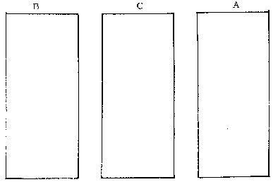
The Master RAM memory is divided into three separate memory banks, called A, B, C. With one restriction each RAM memory may contain 4K or 16K dynamic RAM chips or they may be left empty. This yields a total RAM availability from 8K to 48K bytes,
The addressing of the dynamic RAM is controlled by a single PROM programmed to correspond to the physically present RAM configuration, The exchange of this chip and changing of a switch is the only operation, other than replacement of RAM chips, that is necessary to implement a configuration change. The RAM memory is seen by the program as a continuous block of memory starting at (hex) address 0000 up to a maximum address which for 48K is BFFF.
The first RAM bank, (if present) starts at address 0000 and is available for program use only and may not contain display data, The remaining two banks which must both be present are arranged for 16 bit (two-byte) wide access by the display controller, Bank B contributes the low-order bits, and bank C the high-order bits of the 16 bit word. For processor access even-address bytes are in bank B and odd-address bytes are in bank C, e. g,: if bank A is 4K and occupies addresses 0000 to OFFF then address 1000 is in bank B, address 1001 is in bank C etc. to the end of the Master RAM.

11.
Programmable RAM select Logic
For each RAM configuration of the DAI Personal Computer it is necessary to define the address decoding. This is achieved using a single factory programmable ROM. These are supplied for each defined RAM configuration,
| RAM configuration | Banks B+C address | Bank A |
| 8K | 0000 - 1FFF | not used |
| 12K | 1000 - 2FFF | 0000 - 0FFF |
| 32K | 0000 - 7FFF | not used |
| 36K | 1000 - 8FFF | 0000 - 0FFF |
| 48K | 4000 - BFFF | 0 - 3FFF |
No other aspect of the machine is altered by changes to the RAM configuration,
Master RAM Configurations VS Graphical Capability
| Master RAM Configuration |
Graphical Resolution |
Display Color Modes |
Required Picture Space |
Available Prog. and Work space |
Notes |
| 8K | 65 x 88 | 4 16 | 1.5K | 6.5K | |
| 130 x 176 | 4 16 | 5.8K | 2.2K | ||
| 12K | 65 x 88 | 4 16 | 1.5K | 10.5K | |
| 130 x 176 | 4 16 | 5.8K | 6.2K | ||
| 32K | 65 x 88 | 4 16 | 1.5K | 30.5K | |
| 130 x 176 | 4 16 | 5.8K | Z6.2K | ||
| 260 x 352 | 4 16 | 22.8K | 9.2K | ||
| 36K | 65 x 88 | 4 16 | 1.5K | 34K | |
| 130 x 176 | 4 16 | 5.8K | 30K | ||
| 260 x 352 | 4 16 | 22.8K | 13K | ||
| 240 x 528 | 4 16 | 32K | 4K |
12.
| 48K | 65 x 88 | 4 16 | 1.5K | 46.0K | |
| 130 x 176 | 4 16 | 5.8K | 42.0K | ||
| 260 x 352 | 4 16 | 22.8K | 25.0K | ||
| 240 x 528 | 4 16 | 32 K | 16.0K | non-square |
The above are examples of the RAM requirement for possible all- graphics screen configurations. Actual usage will be affected by the screen driver package used.
ROM and Static RAM Memory
The system software resides in mask programmed ROM’S starting at address C000 and extending to EFFF. Addresses C000 through DFFF are continuous program space while addresses E000 through EFFF have four switchable BANKS of program space. Total program ROM space is therefore 24K bytes. In the address range F800 to F8FF a bank of static RAM is included for use by the 8080A stack, and for a vector of jump instructions that allow the emulation of an MDS system.
13.
Simplified memory map (48K RAM P. C. ).
